You drive a hybrid car and find a special tour through the navigator. You look at the weather forecast on a mobile phone in a sturdy, warm house. You can buy milk from abroad by e-commerce without leaving the house. You sit. Watching the latest 3D movies while eating popcorn in the cinema...
Although we are accustomed to it, our lives have indeed been changed by these once-advanced technologies. In 2015, we guessed who will change us next time?
The reporter learned that the recent high-tech center of the Ministry of Science and Technology, according to the task requirements of the National Soft Science Research Project “Tracking Research on High-Tech Development Trends in the World,†organizes fields such as information, materials, energy, advanced manufacturing, transportation, and basic research. A total of more than 230 experts, experts in the 973 Program, and universities, research institutes, and key enterprises, using a combination of bibliometrics and qualitative analysis, have passed relevant science and technology plans for countries and companies with leading advantages in related fields. The statistical analysis of planning, development and strategic deployment, as well as statistical analysis of relevant academic journals and information in relevant core journals, international academic conferences, etc., proposes a total of 61 current frontier hotspots in all areas.
After further conciseness, they proposed the ten most advanced technologies with the most potential for change.
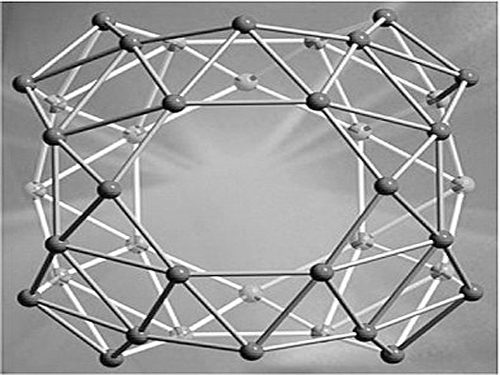
Carbon-based nanomaterials
Carbon-based nanomaterials refer to carbon materials with unique microstructures and properties, including graphene carbon, nanotubes, and carbon quantum dots. Among them, graphene is the thinnest known material at present, with high electrical conductivity, high toughness, high strength, large specific surface area, outstanding thermal conductivity properties; carbon nanotubes have a large aspect ratio, high interface atomic ratio The atomic arrangement is variable and the interfacial lattices are not related to each other; the zero-dimensional carbon quantum dots are different from the traditional toxic quantum dots, and have unique advantages such as environmental friendliness, good biocompatibility, high fluorescence intensity, no flicker, etc. It is also an excellent luminous material.
Carbon-based nanomaterials have become one of the fiercest research areas in the global science and technology and industry competition, and are highly valued by the scientific community, industry, and national governments. With the gradual maturation of different preparation technologies and subsequent application technologies of carbon-based nanomaterials, many traditional and emerging industries will be in the semiconductor industry, photovoltaic industry, new energy storage materials, biopharmaceuticals, composite materials, aerospace, military, and new generation displays. The field brought revolutionary technological changes and became the next petascale industry.
2. Semiconductor nanomaterials
Semiconductor materials that are at least one-dimensional in the three-dimensional space at the nanometer level (less than 100 nm) are called semiconductor nanomaterials. Due to the existence of such effects as size and quantum confinement, semiconductor nanomaterials have unique properties that some bulk materials do not possess. Based on this feature, devices with better performance can be designed and prepared. Therefore, the optimization and application of semiconductor material properties at the nanometer level has always been one of the hot topics in the research of semiconductor materials. At the same time, the cross-convergence of semiconducting nanomaterials and emerging sources such as new energy and biotechnology has also led to a series of new research hotspots.
Semiconductor nanomaterials and technologies are changing the world with unprecedented depth and breadth, and have opened up new levels of understanding of nature in science and technology. The various new principles, new applications, and new devices brought about by semiconductor nanomaterials have greatly enriched and changed the research face of the semiconductor science and triggered new technological revolutions in many fields, becoming one of the most dynamic and high-tech fields in today's world.
3. Optical lithography that breaks the diffraction limit
As the leading and mainstream technology for the manufacture of micro-nano information devices, the development of optical lithography technology is facing a theoretical obstacle: the improvement of the core lithography index of optical lithography is limited by the diffraction limit. Surface plasmon imaging lithography and surface plasma local lithography have become one of the major scientific and technical issues in the field of information in order to overcome the diffraction limit and establish a theoretical hotspot for superresolution imaging lithography theory and technology.
Once these technologies are mature, they can provide optical lithography technology below 32nm, 22nm or even 10nm nodes, which is expected to solve the theoretical and technical dilemma of the international limited diffraction path of traditional lithography technology and become a new optical lithography method and tool.
4. Laser micro-nanometer manufacturing
Laser micro-nano fabrication is an important part of micro-nano fabrication technology. Laser micro-nano fabrication is the interaction of lasers and materials to change the state and properties of materials to achieve micro-to nano-scale or cross-scale control and control. Since the laser micro-nano fabrication can be extreme at the energy density, the space and time scale of action, and the controllable dimensions of the absorbed energy of the manufacturing body, the physical effect and the mechanism of action used in the manufacturing process are completely different from the traditional manufacturing. The ability and quality of manufacturing complex structures is much higher than traditional manufacturing, resulting in a number of new technologies (such as lithography, near-field nanofabrication, interference-induced processing, micro-welding, etc.), and a new batch of products (such as large-scale integrated circuits , MEMS/NEMS, etc.), and a number of high-performance products (such as aero-engines, gas turbines, solar cells, etc.) and corresponding high-tech industrial clusters.
Laser micro/nano fabrication involves disciplines such as optics, physics, materials, chemistry, biology, information, control, mechanics, nanotechnology, etc. It will surely promote the in-depth development of manufacturing and related disciplines. It also provides important manufacturing support for leap-forward development in the fields of energy, aviation, IC manufacturing, defense, automotive, biology, and medical care.
5. Optoelectronic integrated chip technology
Optoelectronic integrated chip technology is a new technology that integrates photoelectric materials and functional microstructures on a single chip to realize system functions. A number of optoelectronic discrete devices, such as lasers, optical modulators, optical detectors, optical amplifiers, and demultiplexers, will be integrated into a single chip through reasonable optimization, design, process processing, and packaging.
Optoelectronic integrated chips can take advantage of high-density integration, low cost, and extremely high photon bandwidth, ultra-fast transmission speed, and high noise immunity, and have outstanding advantages such as low power consumption, high speed, high reliability, and small size. The key links in the fields of transmission, optical information processing and switching, optical access, and optical and wireless convergence play an important role and are the only way to break through the bottleneck of speed and energy consumption of information networks. Optoelectronic integrated chip technology also has broad application prospects in fields such as light sensing, optical computing, biosensing, medicine, and agriculture. It is foreseeable that optoelectronic integrated chip technology will bring about a milestone change in the field of optoelectronics.
6. Post-Moore Era 3D Interconnect Integration and Chip Design
Three dimensional integrated circuit (3DIC) refers to the integration of two or even multiple layers of integrated circuit components into one chip by vertical or horizontal interconnection. The difference between three-dimensional integrated circuits and three-dimensional packages is whether they are integrated into a single chip. Three-dimensional packaging means that multiple chips are packaged in one package, and chips and chips are connected by off-chip interconnections.
Three-dimensional integrated circuits (3DIC) can effectively alleviate the CPU's “storage wall†problem, shorten the DRAM access time by 50 times, greatly ease the limitations of the storage wall, and drive the development of related materials, manufacturing, packaging, and testing technologies. Drive the development of miniaturized integrated circuit application technology, opening the door for automotive electronics, body wearable devices and implantable applications.
3DIC is the root technology of next-generation integrated circuits. It will have an important impact on the miniaturization, low power consumption, and high performance of electronic systems. It may lead to the evolution of CPU and SOC architectures and processes. Packaging and EDA technology innovations. 3DIC has broad prospects for development and application, and will have a profound impact on the smart phone, medical electronics, high-performance computing, Internet of things, automotive electronics, surveillance and security industries.
7. Silicon carbide power electronic device technology
Silicon carbide power electronic devices are different from traditional silicon-based power electronic devices with wide band gaps.
The important system advantages of silicon carbide power electronic devices are high voltage (up to tens of thousands of volts) high temperature (greater than 500°C), which breaks through the limitations caused by voltage (kV) and temperature (less than 150°C) limitations of silicon-based power semiconductor devices. System limitations, so that silicon carbide power electronic devices can meet the energy conversion of high-voltage, large-capacity, high-frequency, high-temperature power semiconductor devices, improve the efficiency of power electronic devices, reduce system losses, to achieve significant energy savings; The volume of various types of inverters in power electronic devices is greatly reduced, which greatly improves the mobility and flexibility of the equipment.
Because of its excellent performance, silicon carbide power electronic devices have been hailed as "green energy" devices that have driven the "new energy revolution" in the 21st century.
8. Quantum Communication Technology and Integration with Classic Communication
Quantum communication, also known as quantum stealth transmission, is a communication method that carries information by the quantum state. It uses the quantum entanglement principle of photons and other elementary particles to realize the secure communication process.
Quantum communication is a new communication method. It is no longer the classical information but the quantum information carried in the quantum state. It is the core element of the future quantum communication network. From a physics perspective, it is possible to visualize the process of stealth transmission by first extracting all the information of the original and then transmitting this information to the receiving location. Based on this information, the recipient selects the basic unit that is identical to the original (eg: Atom) to create a perfect replica of the original. Quantum communication technology is based on the basic principles of quantum physics and overcomes the inherent security risks of classical encryption technology. It is the only communication method that has so far been strictly proved to be unconditional security.
Quantum communication is the first quantum information technology to be practical. Develop and equip quantum communication technologies to realize the integration of quantum communication and classical communication technologies, and substantially increase the national information technology level and the core competitiveness of the information industry, realize the leap-forward development of information system construction, and national defense, finance, and government affairs. Information security guarantees in other fields all play an important role.
9. Track angular momentum communication technology
How the future electromagnetic wave communication technology finds a new dimension of physical parameters, and how to meet the demand for an increase in communication capacity within a limited frequency spectrum resource is a major scientific and technical challenge. It is necessary to find new principles from the physical level. In addition to the angular momentum associated with quantum spins, there is also an OAM (Orbital angular momentum) due to the helical phase structure of the beam. Therefore, OAM is called the final photon (or electromagnetic wave). A basic parameter and has not been applied to communication.
In the aspect of the basic physical parameters of the electromagnetic wave of OAM, it is to explore capacity resources, basic principles, and core technologies that the capacity of the future communication system expands in an order of magnitude, and in combination with the already utilized capacity resources, it is possible to greatly increase capacity. The development of this technology plays an important role in relieving the contradiction between the large-capacity demand of mobile communication systems and the limited spectrum resources and supporting the popularization of mobile Internet.
10. Ubiquitous perception and full distribution control technology
In 1988, Mark Weiser, the father of ubiquitous computing, used the word “ubiquitous†in calculators and networks for the first time. He defined ubiquitous computing as “a method that uses multiple calculators to enhance computing power. At the same time, the user is unaware of how to use it; and predicts the future network model: "The network, like air and water, naturally and deeply integrates into human daily life and work." This is the role of the ubiquitous network.
With the development of wireless technologies, sensing technologies, and chip processing technologies, ubiquitous sensing has become possible. If the ubiquitous network is the highest goal of ICT society development, the Internet of Things is the primary and inevitable development stage of the ubiquitous network, and the sensor network is the extension and application foundation of the Internet of Things.
Ubiquitous perception network is not only a basic network architecture, but also can provide information and communication services to other industries, realize the comprehensive utilization of information, and improve the quality of life and work efficiency of individuals, enterprises, and families; digital and multimedia information services Will be integrated into people's daily work and life, and play a role in facilitating life.
This article refers to the address: http://
1. Features: light LED copper wire falls, there is a kind of like the flowing water of a waterfall effect, waterfall lights as if from top to bottom like huan long splash water, made a bunch of the source of the waterfall model, there is like a perennial small water always pour down, step by step and spacious, with each branch lines of light distance is fixed, so the light effect is very have administrative levels feeling of the waterfall.Lop led twinkle light can according to need to expand (can be neatly like a soft cloth, can also extend to beauty like splash splash, each layer of the emitting light colors are very have administrative levels feeling), waterproof products, energy-saving features.
2. Specifications: Power Supply: Battery box, Electronic, Transformer.Length:
1 m / 2 m / 3 m / 4 m / 5 m are available
LED Color: White warm, White, Amber, Red, Green, Yellow, Blue, Multicolor, RGB.
3. Usage: usage: can use, indoor & outdoor LED copper wire light string not only applied to Christmas lights (e.g., wrapped around the Christmas tree) all kinds of festival holiday decoration, also used for household decoration (can be hung in the window, glass roof, on the corner...To achieve, the icing on the cake) and the city lighting project and various recreational venues, the park (the water effect of the waterfall), all the shopping malls can wait.
Waterfall Lights
Waterfall Lights,Waterfall Curtain Light Outdoor,LED Christmas Waterfall Lights,LED Waterfall Curtain Lights
Heshan Jianhao Lighting Industrial Co., Ltd. , https://www.sunclubtw.com