Ping Pong operation
"Ping-pong operation" is a processing technique that is often applied to data flow control. A typical ping-pong operation method is shown in FIG.
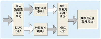
The processing flow of ping-pong operation is: the input data flow distributes the data flow to two data buffers through the "input data selection unit". The data buffer module can be any memory module, and the more commonly used memory unit is dual-port RAM (DPRAM). ), single-port RAM (SPRAM), FIFO and so on. In the first buffer period, the input data stream is buffered to "data buffer module 1"; in the second buffer period, the input data stream is buffered to "data buffer module 2" by the "input data selection unit" switch. "At the same time, the data of the first cycle buffered by the "data buffer module 1" is sent to the "data flow operation processing module" for operation processing through the selection of the "input data selection unit"; the input data is passed through the third buffer cycle. When the selection unit switches again, the input data stream is buffered into the "data buffer module 1", and the data of the second cycle buffered by the "data buffer module 2" is switched over through the "input data selection unit" and sent to the data. "Stream operation processing module" performs arithmetic processing. This cycle.
The most important feature of ping-pong operation is that the input data selection unit and the output data selection unit switch between beats and interactions, and the buffered data stream is sent to the “data flow operation processing module†for operation and processing without stopping. . Looking at the ping-pong operation module as a whole, looking at the data at both ends of the module, the input data stream and the output data stream are continuous and without any pauses, and therefore are very suitable for streamlining the data stream. Therefore, ping-pong operations are often applied to pipelined algorithms to complete seamless buffering and processing of data.
The second advantage of ping-pong operation is that it saves buffer space. For example, in a WCDMA baseband application, a frame is composed of 15 time slots. Sometimes it takes a whole frame of data to be delayed by one time slot. The more direct method is to buffer this frame of data and then delay the time. One slot is processed. At this time, the length of the buffer is one full frame of data. Assume that the data rate is 3.84 Mbps and the length of one frame is 10 ms. In this case, the buffer length is 38,400 bits. If you use ping-pong operation, you only need to define two RAMs that can buffer one time slot (single-port RAM is sufficient). When writing data to a RAM, data is read from another RAM and then sent to the processing unit for processing. At this time, the capacity of each RAM is only 2560 bits, and 2 RAMs add up to only 5120 bits. 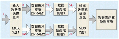
In addition, clever use of ping-pong operation can also achieve the effect of processing high-speed data streams with low-speed modules. As shown in Figure 2, the data buffer module uses dual-port RAM and introduces a data pre-processing module after the DPRAM. This data preprocessing can be based on various data operations required, such as input data in WCDMA designs. Stream despreading, descrambling, derotation, etc. Assume that the input data stream rate of port A is 100 Mbps, and the buffering period of ping pong operation is 10 ms. The following analyzes the data rate of each node port.
The input data flow rate at the A port is 100 Mbps, and it arrives at DPRAM1 from B1 through the “input data selection unit†within 10 ms of the first buffering period. The data rate of B1 is also 100Mbps, and DPRAM1 writes 1Mb data within 10ms. Similarly, in the second 10 ms, the data stream is switched to DPRAM2, the data rate of port B2 is also 100 Mbps, and DPRAM2 is written with 1 Mb data in the second 10 ms. In the third 10ms, the data stream is switched to DPRAM1 again, and DPRAM1 is written with 1Mb data.
After careful analysis, it will be found that when the third buffer cycle is completed, the time for DPRAM1 to read data and send it to “data pre-processing module 1†is a total of 20 ms. Some engineers wondered why DPRAM1's reading time was 20ms. This time came from the following: First, within 10ms of writing data to DPRAM2 during the 2nd buffer cycle, DPRAM1 can perform a read operation; in addition, in the 1st From the 5ms of the buffering period (absolute time is 5ms), DPRAM1 can write data to the address after 500K, while reading from address 0, and when it reaches 10ms, DPRAM1 just finished writing 1Mb data and read 500K data. In the buffer time DPRAM1 reads 5ms; in the 5ms of the 3rd buffering cycle (absolute time is 35ms time), similarly can read data from address 0 while writing data to the address after 500K, read 5 ms again Therefore, before the data stored in the first cycle of DPRAM1 is completely covered, DPRAM1 can read a maximum of 20ms, and the data to be read is 1Mb, so the data rate of port C1 is: 1Mb/20ms=50Mbps. Therefore, the minimum data throughput capacity of "Data Preprocessing Module 1" is only required to be 50 Mbps. Similarly, the minimum data throughput capacity of "Data Preprocessing Module 2" is only required to be 50 Mbps. In other words, through the ping-pong operation, the timing pressure of the "data preprocessing module" is reduced, and the required data processing rate is only 1/2 of the input data rate.
The essence of low-speed module processing of high-speed data through ping-pong operation is that the serial-to-parallel conversion of the data stream is implemented through the DPRAM buffer unit, and the data is processed in parallel by the “data preprocessing module 1†and the “data preprocessing module 2 â€. Is the embodiment of the principle of exchange of area and speed!
Serial-to-parallel conversion design tips
Serial-to-parallel conversion is an important technique for FPGA design. It is a common method for data stream processing and a direct reflection of the idea of ​​area and speed interchangeability. There are many ways to implement serial-to-parallel conversion. According to the requirements of data sorting and quantity, registers and RAM can be used to implement. In the previous example of ping-pong operation, data stream serial-to-parallel conversion was realized through DPRAM, and due to the use of DPRAM, the data buffer can be opened very large. For a relatively small number of designs, registers can be serially converted. If there is no special requirement, the serial-to-parallel conversion should be completed with synchronous timing design. For example, data from serial to parallel, the data is arranged in order of the highest order, can be achieved with the following code: 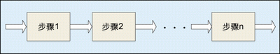
Prl_temp<={prl_temp,srl_in};
Among them, prl_temp is the parallel output buffer register, and srl_in is the serial data input. For a serial-to-parallel conversion with a specified order, you can use the case statement to determine the implementation. For complex serial-to-parallel conversions, it can also be implemented using state machines. The serial-to-parallel conversion method is relatively simple and need not be described here.
Pipeline operation design ideas
The first thing to declare is that the pipeline described here refers to a design concept for processing flow and sequential operation, not "Pipelining" for optimizing timing in FPGA and ASIC design.
Pipeline processing is a common design method in high-speed design. If a design's processing flow is divided into several steps, and the entire data processing is "single flow", ie there is no feedback or iterative operation, the output of the previous step is the input of the next step, then the pipeline design method can be considered. Increase the operating frequency of the system.
The schematic diagram of the pipeline design is shown in Figure 3. The basic structure is: the n flow steps of the appropriate divisions are connected in series. The biggest characteristic and requirement of pipeline operation is that the processing of data flow at each step is continuous from the time point of view. If the simplifying of each operation step is assumed to be through a D flip-flop (that is, one cycle with a register), then the pipeline operation is performed. Like a shift register bank, the data stream flows through the D flip-flops in turn, completing each step of the operation. The pipeline design timing is shown in Figure 4.
A key to pipeline design is the rational arrangement of the entire design sequence, which requires a reasonable division of each operation step. If the pre-stage operation time is exactly equal to the post-stage operation time, the design is the simplest, the output of the pre-stage can be directly imported into the input of the post-stage; if the pre-stage operation time is greater than the post-stage operation time, the output of the pre-stage is required. The data is properly buffered before it is imported into the input of the next stage. If the operation time of the previous stage is just smaller than the operation time of the later stage, the data stream must be split by the replication logic, or the data must be stored and processed at the preceding stage. Otherwise, the data is processed. It will cause overflow of data at the later stage.
Pipeline processing methods such as RAKE receivers, searchers, and preamble acquisition are often used in WCDMA designs. The reason why the frequency of pipeline processing is higher is because it duplicates the processing module, which is another embodiment of the idea of ​​area exchange speed.
Data interface synchronization method
Synchronization of data interfaces is a common problem in FPGA/CPLD design, and it is also a key and difficult point. Many design instabilities originate from synchronization of data interfaces.
In the circuit design phase, some engineers manually join the BUFT or non-gate to adjust the data delay, so as to ensure that the clocks of the current module set and maintain the data of the upper module. Some engineers have generated a lot of clock signals with a phase difference of 90 degrees in order to have stable sampling. Sometimes, they use the positive edge to hit the data, and sometimes use the negative edge to hit the data to adjust the sampling position of the data. Both of these practices are extremely undesirable because sampling implementation must be redesigned once the chip is updated or migrated to other chipset chips. Moreover, these two practices result in insufficient circuit implementation margins. Once the external conditions change (eg, temperature increases), the sampling timing may be completely disordered, causing circuit defects.
The following briefly describes the synchronization method of the data interface in several different situations:
1. How to complete the data synchronization under the conditions of input and output delay (chip-to-chip, PCB layout, delay of some driver interface components, etc.) that cannot be measured, or may be changed?
For data delays that cannot be measured or changed, a synchronization mechanism needs to be established, and a synchronization enable or synchronization indication signal can be used. In addition, data can be synchronized through RAM or FIFO access. 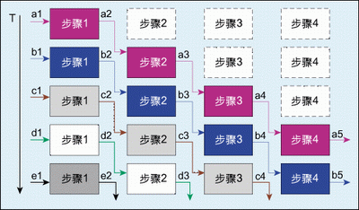
The method of storing data in RAM or FIFO is as follows: the data provided by the upper chip is regarded as a write signal with the channel clock, and the data is written into RAM or FIFO, and then the data is used by the sampling clock of this stage (generally, the main clock of data processing). Read it out. The key to this approach is that data is written to RAM or the FIFO is reliable. If synchronous RAM or FIFO is used, it is required that there should be a route indication signal with a fixed relative delay relationship with the data. This signal can be a valid indication of data, or it can be It is the clock that the upper module clocks out the data. For slow data, asynchronous RAM or FIFO can also be sampled, but this is not recommended.
Data is arranged in a fixed format. Many important information is at the beginning of the data. This situation is very common in communication systems. In communications systems, much of the data is organized in "frames." Because the entire system has a high requirement for the clock, a clock board is usually designed to complete the generation and driving of a high-precision clock. And the data has a starting position, how to complete the data synchronization, and find the "head" of the data?
The data synchronization method can use the above method completely, adopt the synchronous indication signal, or use RAM, FIFO cache. There are two ways to find the data header. The first one is very simple. It can transmit an indication signal of the start position of the data. For some systems, especially asynchronous systems, a synchronization code is often inserted in the data (such as training. Sequence), the receiving end can detect the "head" of the data after the state machine detects the synchronization code. This is called "blind detection".
The upper-level data and the current-level clock are asynchronous, that is, the clocks of the upper-level chip or module and the current-level chip or module are asynchronous clock domains.
In the previous input data synchronization has been briefly introduced a principle: If the input data beat and the same level of chip processing clock, you can directly use the main chip of the chip input data register sampling to complete the input data synchronization If the input data and the processing clock of this stage chip are asynchronous, especially when the frequency does not match, only the register data is sampled twice by the processing clock on the input data to complete the synchronization of the input data. It should be noted that the data of the asynchronous clock domain is sampled twice by the register, and its role is to effectively prevent the propagation of the metastable state (data state instability), so that the data processed by the subsequent stage circuits are all valid levels. However, this method does not guarantee that the data after the two-stage register is sampled is the correct level. In this way, the processing generally generates a certain amount of error level data. So it only applies to functional units that are insensitive to small errors.
In order to prevent the asynchronous clock domain from generating erroneous sampling levels, RAM and FIFO buffers are generally used to perform data conversion in the asynchronous clock domain. The most commonly used buffer unit is DPRAM, which uses the upper clock to write data at the input port and the current clock at the output port. This facilitates the exchange of data between the asynchronous clock domains.
2. Does design data interface synchronization need to add constraints?
It is advisable to add appropriate constraints, especially for high-speed designs. It is necessary to add corresponding constraints on the cycle, setup, and hold time.
There are two points to the effect of the additional constraints here:
a. Improve the working frequency of the design to meet the interface data synchronization requirements. Logic synthesis, mapping, placement, and routing can be controlled through additional cycle, setup, and hold time constraints to reduce logic and routing delays, thereby increasing operating frequency and meeting interface data synchronization requirements.
b. Obtain the correct timing analysis report. Almost all FPGA design platforms include static timing analysis tools that can be used to obtain timing analysis reports after mapping or placement and routing to evaluate the performance of the design. Static timing analysis tools use constraints as a criterion to determine whether the timing meets the design requirements. Therefore, the designer is required to input the constraints correctly so that the static timing analysis tool can output the correct timing analysis report.
Common constraints related to Xilinx and data interfaces include Period, OFFSET_IN_BEFORE, OFFSET_IN_AFTER, OFFSET_OUT_BEFORE, and OFFSET_OUT_AFTER. Altera's common constraints related to data interfaces include Period, tsu, tH, and tco.
MC Flex Indoor Rental LED Display
Advantage of Indoor Rental LED Display P3.91 P4.81
1. Lightweight. Convenient in transporting and installing & saving labor cost, suitable for flow shows.
2. Nice appearance and simple structures.
3. Jointed correctly, being installed & dismounted by one person without tool.
4. Humanized operating interface with breakdown indicator lights, easy to maintain.
5. High debugging brightness and no damage to gray scale, achieving the debugging technology for nice image.
Indoor Rental LED Display
Indoor Rental LED Display,Indoor Rental LED Screen,Indoor Rental LED Screen Display,Indoor Stage Rental LED Display
Shenzhen Macion Optoelectronics Technology Co.,Ltd. , https://www.macion-led.com