1, electronic ballast
Electronic ballast (Electrical ballast), a type of ballast, refers to an electronic device that uses electronic technology to drive an electric light source to produce the desired illumination. Corresponding to this is an inductive ballast (or ballast). Modern fluorescent lamps are increasingly using electronic ballasts, which are light and compact, and can even integrate electronic ballasts with lamps. At the same time, electronic ballasts can usually have a starter function, so it can save Go to a separate starter. The electronic ballast can also have more functions, such as improving or eliminating the flickering of the fluorescent lamp by increasing the current frequency or current waveform (such as becoming a square wave), or using the DC power supply by the power inverter process.
2, the composition of the electronic ballast
The electronic ballast is composed of anti-interference filter, rectification and filtering circuit, power factor adjuster, high frequency conversion, resonant circuit, abnormal state protection circuit and fluorescent lamp. The functions of each part are as follows:
1) Anti-interference filter: Prevents high-frequency interference signals generated by electronic ballasts from entering the grid and causing radiation.
2) Rectifier filter circuit: convert 220V power frequency (50Hz or 60Hz) AC power into 310V DC power, as the power source of electronic ballast.
3) Power factor adjuster: adjust and compensate the power factor of this unit.
4) High-frequency conversion circuit: The heart circuit of the electronic ballast converts the DC power supply into a high-frequency power supply of about 20K to 50KHz to drive the fluorescent lamp. This circuit is usually implemented by a self-excited oscillator consisting of a pair of power transistors (triodes or field effect transistors).
5) Resonant circuit: A starter used to replace ordinary fluorescent lamps. It can be equivalent to a series resonant circuit before the fluorescent lamp illuminates. Its oscillation frequency is consistent with the frequency of the high-frequency conversion circuit. At resonance, on the capacitor C. A very high voltage is generated to ensure that the lamp is lit. The lamp is lit and its equivalent resistance is reduced. This resistor is connected in parallel with the capacitor C, which greatly reduces the Q value of the resonant circuit. The circuit becomes an RL series circuit, and L becomes a current limiter.
6) Abnormal state protection circuit: When the fluorescent lamp is not normally lit, a high resonance voltage will burn the power device. The function of this circuit is to protect the power device from burning in an abnormal state.
7) Fluorescent lamp: The function is to convert high-frequency electric energy of about 20K to 50KHz into light energy.
3. Sources and effects of electromagnetic interference in electronic ballasts
3.1. Sources of conducted interference and their effects
The electromagnetic noise generated by the electronic ballast is transmitted to the power grid through the input power line, causing conducted interference, causing pollution to the surrounding environment and affecting the normal operation of the related electronic equipment or system. Electronic ballast
Conducted interference sources mainly come from the following aspects:
(1) The inherent noise of components. There are mainly thermal noise, shot noise, and contact noise.
(2) Electromagnetic noise generated by the semiconductor diode during the switching process. At the same time of rapid turn-on and turn-off, transient voltages and currents form strong electromagnetic noise.
(3) Power semiconductor devices generate high transient voltages or currents and cause oscillation during switching. The faster the switching speed, the larger the switching current, and the greater the transient electromagnetic noise caused. Power semiconductor devices generate direct conducted interference on the AC grid, which is differentially modeled and common mode.
(4) In the passive power factor correction structure using the high frequency pump or the double pump circuit, the high frequency switching signal of the power switch tube is applied to the input terminal through the feedback component, and is sent into the power grid through the power supply line to form conducted interference.
3.2. Sources of radiation interference and their effects
When the electronic ballast is working, the magnetic field and electric field formed are radiated outward in the form of electromagnetic waves through the input and output wires and loads or some components, and the disturbance formed by electromagnetic waves between the surrounding electronic and electrical equipment is called radiation. interference. Radiation interference mainly exists in the form of a magnetic field, which is caused by the magnetic field and is caused by the mutual inductance between the conductors. When the current in the circuit is abrupt, the flux that is connected to the circuit changes, and the interference voltage is induced.
3.3, the source of harmonic interference and its impact
Since the load of the electronic ballast is a non-linear load, harmonics are generated during operation. In addition, low power factor circuits or power factor correction circuits dispose of improper electronic ballasts whose output current waveform will produce severe harmonic distortion. Harmonic effects and hazards are mainly manifested in: increasing circuit losses, increasing temperature rise, reducing efficiency and service life; increasing dielectric loss and partial discharge in insulation, accelerating insulation aging; increasing noise.
4. Inhibition measures for electromagnetic interference of electronic ballasts
4.1. Conductive interference suppression measures
1) Reasonable grounding
Conducted interference is generated by the common grounding of the electronic ballast and the common impedance in the grounding network. Grounding should be reasonably arranged, the ground wire should be as short as possible, and the input ground and the output ground should be separated, and the independent ground wire should be connected in parallel.
The grounding method of the point, which can prevent the conductive coupling between the grounds and reduce the interference between the control signals. The grounding of the casing can achieve shielding of the electric field, and the shielding can weaken the interference to the internal and external circuits. For example, the phase and neutral lines of the power supply can be connected to the casing and the earth through the Y capacitor to reduce the conducted interference noise of the system.
2) Add a decoupling circuit to the DC power supply circuit
The RC decoupling circuit is added to the switching tube power supply circuit so that the current required for the opening of the switching tube is no longer provided by the power supply, and the decoupling capacitor provides a current compensation source for the device to reduce the power supply and grounding system.
The noise caused by the current fluctuations. In addition, in the half-bridge inverter circuit of the electronic ballast, the capacitance connected between the midpoint of the half bridge and the ground can reduce ΔU/Δt and △I/Δt, which helps to suppress electromagnetic interference noise. .
3) Using passive filters
The use of passive EMI filters is the most effective way to suppress conducted interference. That is, a band-pass filter is inserted in the circuit to make the 50 Hz AC unblocked, and the signals of the remaining frequencies are blocked. However, it is necessary to strictly control the parasitic parameters of the LC components of the filter. Their fabrication process, mounting position, and routing method will affect the EMI filtering effect. Adding the filter circuit shown in Figure 1 can control the level of noise entering the grid through conduction coupling.
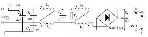
Figure 1 EMI filter circuit
The output of the filter is connected to the noise source, and the input is connected to the grid to prevent various high frequency and transient noise from entering the grid through conduction. The effect of the filter to suppress electromagnetic noise can be measured by the insertion loss: the larger the insertion loss, the better the filtering effect and the greater the suppression of conducted interference.
Conducted interference mainly manifests as differential mode interference and common mode interference.
(1) Common mode interference suppression

Figure 2 Filter with common mode choke
The common mode choke is an inductive component that plays a dominant role in common mode insertion loss. According to the principle of electromagnetic induction, in Fig. 2, since the common mode currents (Icm and I'cm) are the same, the magnetic lines of force formed in the magnetic ring are superimposed one another, that is, the magnetic fluxes are superimposed on each other. Since the magnetic flux Ф = LI, the total inductance of the common mode choke is L = (Ф1 + Ф 2) / Icm. If the common mode choke is serially connected in the circuit, it is equivalent to a low-pass filter component in the circuit, which plays a common mode suppression effect.
(2) Differential mode interference suppression
The differential mode choke is an inductive component that plays a leading role in differential mode insertion loss. It is wound by a single winding structure, and the signal current on the line also generates a certain amount of magnetic flux in the magnetic ring, so it is easy to achieve saturation. Therefore, the differential mode choke inductor value is small, and the order of magnitude is generally μH. The common mode choke adopts two identical winding structures on one core. The currents of the two windings are opposite in direction, and the magnetic flux generated by the signal current in the magnetic ring cancels each other, so there is no magnetic saturation phenomenon. Therefore, the inductance value can be large, and the order of the common mode magnetic ring is generally mH.
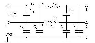
Figure 3 Filter with differential mode choke
According to the principle of electromagnetic induction, in FIG. 3, due to the action of the differential mode currents (Idm and I'dm), a magnetic flux is generated in the magnetic ring, thereby generating an inductance, so that a low-pass filter element is inserted in the circuit, thereby Played a differential mode suppression. Of course, since Icm also generates magnetic flux, which in turn generates inductance, the differential mode choke coil also suppresses common mode interference, but suppressing common mode interference requires a large inductance, and the inductance generated by the differential mode choke coil. Smaller, so the suppression of common mode interference is small.
Similarly, according to the principle of electromagnetic induction, since the differential mode currents (Idm and I'dm) are opposite in direction, the magnetic lines of force formed in the magnetic ring cancel each other out, that is, the magnetic fluxes cancel each other out, so the common mode choke pair differential mode Current five inhibition. In actual production, since the two wires (1 and 2) are impossible to achieve complete balance (incomplete symmetry of lead length and leakage inductance), there is an unbalanced inductance Le, and the value of Le is generally smaller than L/100. Therefore, the common mode choke also works for differential mode interference, but the effect is small.
The above passive EMI filter is reciprocal, which can suppress electromagnetic interference of the electronic ballast from being sent into the power grid, and can also prevent electromagnetic interference in the power grid from entering the electronic ballast.
The component parameters of the EMI filter with common mode inductance cannot be calculated by the formula obtained by the filter without mutual inductance. It is usually necessary to first determine the circuit structure used, and then use the common mode equivalent circuit to find its common mode insertion loss using the network analysis theory.
4.2. Inhibition measures for radiation interference
1) Shielding
Although the electronic ballast itself generates radiation interference, and the output wire and the lamp tube also generate radiated electromagnetic interference, it can be reliably grounded by placing the electronic ballast into the metal shielded casing with the grounding point and the metal casing of the lamp. solve. Shielding is the most effective way to reduce radiation interference.
2) Isolation
Radiation interference generated by the internal circuitry of the electronic ballast interferes with other lines through electromagnetic coupling in the form of an electromagnetic field around the circuit. The easiest and most effective way to prevent this interference is to isolate the electronic ballast from other lines, cutting or weakening the electromagnetic coupling between them. The principles and methods of isolation are:
(1) Interference lines and other lines should not be arranged in parallel as much as possible;
(2) The sensitive lines are arranged in parallel with the general lines, and the spacing should be greater than 50 mm;
(3) The power feeder and signal line should be isolated.
4.3. Harmonic interference suppression measures
It is often contradictory to suppress the current harmonic content and reduce the lamp current crest factor. The contradiction between these two parameters can be solved by active power factor correction technology. However, electronic ballasts using PFC, when plugged
After entering the EMI filter network, it may have certain influence on the input current harmonic total (THD), input power factor (PF) and lamp current peak ratio (CF).
Hifi Earbuds,Best Hifi Earbuds,Hifi In Ear Headphones,Best Hifi Earphones
Dongguang Vowsound Electronics Co., Ltd. , https://www.vowsound.com