Summary
The jitter indicator is one of the most important key parameters when selecting a clock device. However, different clock devices have different descriptions of jitter. For example, a clock driver without a phase-locked loop has additional jitter specifications, while a clock driver with a phase-locked loop for zero delay has periodic jitter and inter-cycle jitter. . At the same time, different manufacturers have different definition conditions for the jitter indicators of the relevant clock devices, such as testing under the condition of a clock synthesizer or testing under the condition of jitter filtering.
In order to correctly understand the jitter specification of clock-related devices and select the clocking solution for the system application, this article details how to understand the jitter parameters of the two types of clock drivers, and understand the clock device from the phase-locked loop output noise characteristics. Noise characteristics of the synthesizer and jitter filtering function.
1 Overview
With the increase of semiconductor process speed and integration, and the improvement of analog integrated circuit design capability, the product form of phase-locked loop chip is more and more abundant, which greatly improves the flexibility of system clock scheme design and reduces the total system clock scheme. cost. At present, phase-locked loop integrated chips have been widely used in wireless communications, data networks, consumer electronics, medical equipment and security surveillance, enabling communication network timing synchronization, clock generation, clock recovery and jitter filtering, frequency synthesis and conversion. , clock distribution and driver functions.
In the face of a wide variety of chips provided by clock device suppliers, it is a difficult problem for circuit designers to choose a clock circuit that satisfies the performance specifications for the system design while the overall solution cost is competitive. Since the key indicator of the clock device is the jitter specification, the high-performance jitter index is often much higher. This article starts with analyzing the jitter specification of the clock device, and details how to correctly understand the meaning of the indicator in the clock chip device manual. Based on the jitter metrics, a series of clock devices from Texas Instruments (TI) and their jitter performance are introduced to help circuit designers choose the clock solution that works best for them.
2 Clock jitter and phase-locked loop noise model
For clock devices, jitter and phase-locked loops are the two most basic concepts.
2.1 Jitter
As shown in Figure 1, clock jitter can be divided into three types of jitter: TIIE Interval Error, Periodic Jitter, and Cycle to Cycle Jitter. The period jitter is the result of statistics and measurement of the changes of the clock period in multiple periods. The jitter between adjacent periods is the result of the statistics and measurement of the period difference of the clock adjacent period, since the two types of jitter are single periods or phases. The deviation of the adjacent period is characterized by short-term jitter behavior. The time interval error, also known as phase jitter, refers to the offset of the edge of the signal from the ideal time position during level shifting, which is usually characterized by long-term jitter behavior.
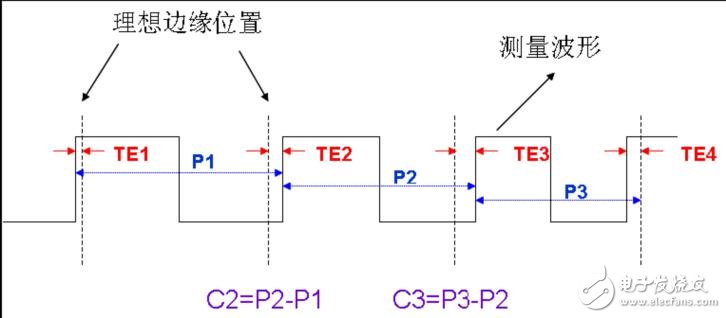
Figure 1 Jitter definition
From the source analysis of clock jitter, jitter can be grouped into two broad categories: deterministic jitter and random jitter. Deterministic jitter is caused by various identifiable interfering signals, such as EMI radiation, power supply noise, synchronous switching noise, etc., which is bounded and can be eliminated or substantially reduced by circuit design optimization. Generally, the jitter performance of the clock device is not directly described. Random jitter is an unpredictable source of noise, such as thermal noise (also known as Johnson noise or shot noise), and the limitations of semiconductor processing. Since random noise is superimposed by a variety of uncorrelated noise sources, Gaussian distribution can be used to describe its characteristics according to statistical theory, so that the following two kinds of representations of random jitter amplitude can be obtained:
1. Mean (RMS) jitter, which is the Gaussian distribution first-order standard deviation value s. RMS jitter within the specified filter bandwidth is typically used, as is commonly used in the field of optical communications (12KHz ~ 20MHz).
2. Peak-to-peak jitter, which is the difference between the smallest measured value and the largest measured value on the Gaussian normal curve. According to the data system error rate requirements, the minimum and maximum values ​​are different, such as the bit error rate.  When the peak-to-peak value is approximately equal to 14 times the standard deviation value,
  .
.
2.2 Phase noise
Phase noise is a frequency domain representation of the noise characteristics of the clock signal. The stability of the frequency of the clock signal is the ratio of the noise power to the total power of the carrier signal within 1 Hz of the carrier frequency (f-fc). The symbol is L ( f), the unit is dBc/Hz. Figure 2 shows the spectral characteristics of a clock signal. If the single-frequency signal is very stable, its sideband will gradually decrease with the position away from the main frequency. At the offset carrier (f-fc), the phase noise is approximately equal to The difference between the height of the curve at the carrier frequency and the height of the curve at f, ie L(f-fc) in the figure
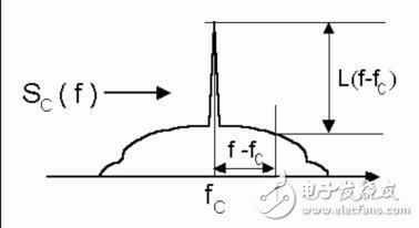
Figure 2 Phase noise definition
2.3 Mean jitter and phase noise relationship
Through the previous analysis, the noise can be characterized by the phase jitter index of the time domain and the phase noise index of the frequency domain, but the two reflect the same physical phenomenon, so the mean jitter can be calculated by the phase noise curve in the frequency domain, according to the relevant literature. The relationship between phase noise and mean jitter in the frequency domain is as follows:
 (1)
(1)
Note: f1 and f2 are the upper and lower limit frequencies of the jitter integral, and f0 is the signal center frequency.
The following is a specific example to illustrate how the spectral density curve in the frequency domain is converted to the jitter value in the time domain.
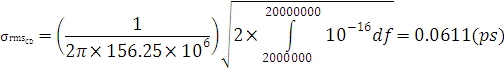
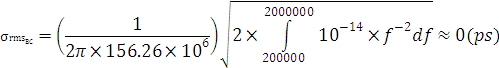
Figure 3 shows the phase noise of a phase-locked loop clock device output. The carrier frequency Vo = 156.25MHz. For the convenience of calculation, the phase noise curve is approximated to the red curve segment in the figure. The AB and CD segments are constant.  dBc/Hz, BC segment 20dBc attenuation, power rate is approximately
  The type of noise.

Figure 3 phase noise curve
According to the conversion relationship between phase noise and mean jitter, the de-integration frequency ranges from 12KHz to 20MHz.
Approximate equivalent mean jitter of the AB segment (12KHz ~ 200KHz)
Approximate equivalent mean jitter for CD segments (2MHz ~ 20MHz)
Approximate equivalent mean jitter of BC segment (200KHz ~ 2MHz)
The total equivalent mean jitter is: 
Food Processor 10 In 1 is one of the most popular model among our Food Processors. They include almost all the features that can meet the needs of family life.
Description for Food Processor 10 In 1
400W
1.0L glass jar blender, grinder, juicer, citrus, juicer, mixer, meat mincer
2 speeds with pulse
shink bag packing
Color box: 66*24.5*44.5cm
40'HQ: 970pcs

Food Processor 10 In 1
Food Processor 7 In 1,Food Processor Blender Juicer,Electric Stainless Steel Food Processor,Electric Vegetable Food Processor
Flying Electronic Co., Ltd , https://www.flyingelectronic.com