As a third-generation display, known as a fantasy display, the organic electroluminescent device (OLED) has active illumination, fast response, high brightness, full viewing angle, DC low voltage drive, all solid state, and is not susceptible to environmental influences. Such excellent characteristics, with the advantages that LCD can't match, have broad application prospects in mobile phones, personal electronic assistants (PDAs), digital cameras, car displays, notebook computers, wall-mounted TVs and military fields, and thus have received wide attention in the industry. The development of OLED has been developed from the original monochrome to the current full color. At the same time, higher requirements are placed on the driver circuit, from the initial gray-free monochrome static drive to the color dynamic drive.
At present, the research focus of OLED is to develop high-stability devices to meet practical requirements, but it is also important to study the driving technology for achieving high-quality dynamic display, because only a good combination of driving technology can improve the reaction speed and resolution. In order to show the excellent characteristics of OLED. However, the monochrome OLED display requires a higher control precision of the driving voltage, and the color OLED display is more difficult to implement in order to accurately control the gradation of the RGB three primary colors at the same time. In order to achieve true color, the three primary colors of R, G, and B should each achieve 256 gray levels. The circuit described in the paper belongs to the full-color dynamic driving circuit, and will study and design its 256-level gray scale display and peripheral drive, which will provide a feasible technical solution for large-size OLED displays in the future.
1 drive control system designThe performance of the display depends on the material of the display on the one hand and the drive circuitry of the display on the other hand. The drive circuit system is an indispensable part to ensure the normal operation of the display, and plays an important role in the display performance. The difference of the drive circuit system will cause the display to display color, brightness, display gray level, response time, power consumption and other display parameters. The OLED display requires a dedicated control driver chip. Only the successful combination of the OLED panel and the driver control chip can promote the development of OLED and replace the LCD. However, the hotspots of OLED research at home and abroad are mainly on devices and materials. There are relatively few studies on circuit and gray scale control, the existing OLED drive circuit has low integration, and the scanning efficiency optimization for OLED characteristics is not high. Therefore, designing a high-performance OLED driver circuit has become an urgent problem to be solved in the display field. Based on the existing research, the paper designs a peripheral drive circuit with resolution of 480 & TImes; 640 color OLED screen, and optimizes the 256-level gray scale implementation method to make it perfectly integrated with OLED, thus further promoting OLED orientation. Pre-development.
1. 1 OLED pixel unit circuitFor the implementation of the OLED drive control system, the key technology is data writing and scanning control. Figure 1 is a single-pixel dual-tube drive circuit. One TFT is used for addressing and the other is a current-modulating transistor that supplies current to the OLED. To prevent current changes due to changes in the OLED turn-on voltage, a P-channel device is used so that the OLED is at the drain of the drive TFT and the source voltage is independent of the voltage across the organic layer.
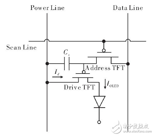
Figure 1 OLED double tube drive circuit
The Data Line is connected to the source of the addressing TFT. The Scan Line gates the address TFT. The contents of the data line are written to the storage capacitor CS by leakage current and temporarily stored as a charge.
When Power Line is high, the source level of the driving TFT is high, and the charge on CS will gate the driving TFT, and its leakage current flows through the OLED display device to drive its light. The level of the data line determines the brightness and darkness of the pixel.
1. 2 256 levels of grayscale displayThe gray level of the image refers to the level of the brightness of the image, and the brightness of the base color is divided by the intensity, which is the gray level.
The higher the gray level that the display can produce, the more colors and image levels are displayed. Moreover, the perception of the brightness of the human visual system is not only related to the intensity of the brightness itself, but also related to the lighting time and the lighting area. In a certain time range, the longer the lighting time, the larger the area, the human eye feels. The stronger the luminous intensity. Therefore, by using the "suspend" effect that the human eye is not sensitive to fast bright and dark flicker, changing the lighting time and area of ​​the illuminant to distinguish the brightness, a different gray level picture is formed, and the general gray level is formed. The higher the color and image level displayed, the softer the image and the more realistic the image hierarchy. High gray level and effective gray level modulation are extremely important for the development of high definition display. At present, an OLED display driver needs to solve the problem of gray scale accuracy.
The OLED display can achieve gray scale by the traditional analog voltage control method. The problem is: There is a nonlinear relationship between brightness and data voltage, and there is a gradual and easy-to-control linear interval. Therefore, the analog voltage method is used to adjust the luminous intensity. It is difficult to accurately and efficiently achieve gray scale display of OLEDs, and the general trend now is to use digital drive circuits.
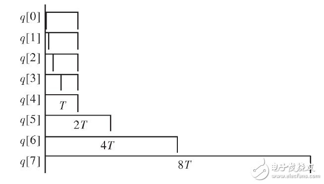
Figure 2 shows the time-sharing diagram
The difficulty of the digital driving circuit is that the operating frequency is much higher than that of the analog driving circuit. There are two main practical gray-level modulation methods at this stage. One is the pulse width modulation method, that is, the control of the duty cycle of the driving pulse; the other method is the subfield control method, which divides the illuminating time into several subfields by 1: 2: 4: 8: ... Different subfields can be combined to achieve different gray levels. However, the pulse width modulation method has a complicated timing, and the display screen has a higher response speed. However, the subfield method requires a higher driving frequency, which is difficult to implement for a high gray level.
Considering the compromise between frame rate and OLED screen display efficiency, the operating frequency of the driver circuit is at a reasonable level. Based on the pulse width modulation and subfield principle, the two methods are optimized, and 256 gray scales are adopted. The image data is implemented by the method of bit time division display, that is, for the input 8 bit pixel signal RGB, the gray display is achieved by assigning different display times to different bits of each color byte, so that the display time of each bit is 128: 64: 32: 16: 8: 4: 2: 1, using the combination, the sub-pixel illumination time corresponding to the 256-level gray scale display can be obtained, and the visual 256-level gray scale is 16.67 million color display, Achieve high quality display.
To achieve 256 levels of gray, the scan time of one pixel is divided into 19 unit time t, and the time taken by the 8 bit gray data q[7: 0] from high to low is 8t, 4t, 2t, t , t, t, t, t. In order to make the display time of different bits into a certain proportion, the erasing time of t /2 is introduced from q[3], q[2] introduces the erasing time of t /4, d[1 Introducing the erasing time of t / 8, d[0] introduces the erasing time of t /16, as shown in Figure 2, the blanking signal is generated by the control circuit for blanking. Calculate the OLED screen brightness percentage λ = ( 8 + 4 + 2 + l + 1 /2 + 1 / 4 + 1 / 8 + 1 / 16 ) / 19 = 83. 9%.
1. 3 FPGA ControllerUtilizing the processing speed and data width of the FPGA and the abundant resources available in the chip, the peripheral drive control circuit is designed for the OLED display with resolution 480 & TImes; RGB & TImes; 640. Its main function is to provide scanning control signals to the OLED display and digital signal processing for OLED display data.
According to the structure and characteristics of the peripheral interface of the OLED display, the FPGA chip is used to design a peripheral drive control system to provide control signals for the OLED screen and to transmit the data signals to be displayed.
As shown in Figure 3, the decoded image data is stored in the FIFO (First In First Out) buffer. Under the control of the main clock, the image data in the FIFO is loaded into a 16 × 8 data load register. When the 16 8-bit data load registers are full, they will be latched by a 144-bit latch and wait for the D/A converter module. At the same time, the FPGA controller will also generate a row-column shift clock under the control of the master clock. And the row and column scan start pulse, the generated clock and pulse enter the DC-DC conversion module.
Figure 3 shows the block diagram of the FPGA controller.
1. 4 various control signal periods and frequenciesIn order to enable the FPGA controller to operate at a reasonable drive frequency and increase the brightness of the display, the structure is in the form of standard cell blocks. For a display with a resolution of 480 × 3 × 640, a unit block is formed by 8 × 16 display pixel tubes, and 480 × 3 rows are grouped into 90 blocks, that is, each block is composed of a group of column signals simultaneously. Drive 16 rows of pixels. When designing the column scan driver circuit, 640 column electrode groups are combined into 80 blocks, each of which drives 8 columns of pixels in parallel.
The refresh rate of the OLED display is 60 Hz / s, that is, the time for displaying one frame of image is 1 / 60 s, set to T, so the period T of the line scan start signal stx is 16 667 μs, and the duty ratio is 1. : 90; Because the 480 × 3 row electrode group of the OLED display is combined into 90 blocks, the gate time of each block is T / 90, which is 185. 185 μs. And cpx and cpbx are a pair of inverting non-overlapping Pulse signal, the duty cycle is 50%. When the pulse signal is high level and low level, there is a block line pixel strobed, that is, two block line pixels are strobed in one cycle of cpx and cpbx, so The period of the line scan drive pulses cpx and cpbx is T / 45, which is 370. 370 μs.
Similarly, the column of the OLED display is divided into 80 blocks, the gate time of each column block is 2.315 μs, the period of the column scan start signal sty is 185. 185 μs, the duty ratio is 1: 80. The column drive pulses cpy and cpby are also a pair of inverted non-overlapping pulse signals with a duty cycle of 50%. When the pulse signal is high and low, a block is gated. Since the strobe time of each column block is 2.315 μs, the period of the column scan drive pulses cpy and cpby is 4.630 μs.
During each column block strobe, eight 8-bit data read in parallel from the FIFO enters the data latch latch. The data is latched once during each BLOCK strobe, so the data latch signal Lock has a period of 2.315 μs. This is done when 16 8-bit data load registers are full of data. The latching of the data, so the period of the 16-bit shift register clock clk_reg is 0. 145 μs. The speed of reading data from the FIFO must be the same as the speed of loading data into the data load register, then the read clock clk of the FIFO The period of _ fifo is also 0. 145 μs. Approx. 7 MHz for 0. 15 μs ( 6. 896 MHz), so the basic clock of the system is 14 MHz, which is generated by the external crystal of the FPGA. The read clock is divided by two of the base clock.
1. 5 FPGA WorkflowThe FPGA processor is the core part of the design. The workflow is to read 8 8-bit pixel data in parallel from 8 FIFO buffers per clk_fifo clock cycle. When the rising edge of clock clk_reg arrives, 16-bit shift The register is shifted, and its output is connected to the chip select terminals of 16 8-bit data load registers, so that 16 8-bit data load registers are gated one by one, and the data can be loaded into 16 8-bit data loads. In the register, the output of these 16 8-bit registers is connected to the input of the 144-bit latch. After the 16 clocks cllk_reg rising edge, the 16 8-bit data load registers will be loaded in sequence. At this time, the data latch signal Lock arrives, 144 data is latched into the 144-bit data latch, and then the data enters. Go to the DA conversion module, convert it into 16 analog quantities, send it to the OLED display, and load a block data.
Under the control of the column scan drive pulses cpy and cpby, 80 blocks are sequentially gated, and each block is gated, and 144 data shift registers and latches are performed, when 80 blocks are locked. After the save, the loading of one line of data is completed. When the 80 blocks of the first row of data are displayed, the column scan start signal sty comes over and starts scanning from the first column. At the same time, under the action of the line scan drive pulses cpx and cpbx, the second row of pixels is Strobe, so, the data loading of 1 to 80 blocks in the second line will be performed, and so on, until the 90 lines of data are displayed, the line scan start signal stx arrives, and the first line is re-strobed. , looping back and forth, displaying data in one frame.
2 simulation resultsAltera's Cyclone III series chip EP3C10E144C8 was selected as the target chip, designed in Verilog HDL language, and Modelsim simulation was performed on GX-SOPC-EDA-EP3C10-STARTER-EDK development board. The simulation results are shown in Figure 4 and Figure 5.
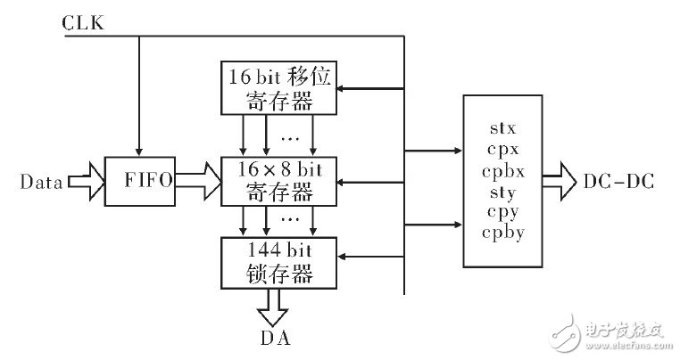
Figure 4 peripheral drive timing simulation results
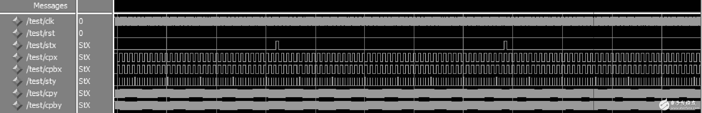
Figure 5 256 grayscale generation simulation
It can be seen from the simulation results in Fig. 4 that 80 sets of scan pulses cpy and cpby control 80 blocks, and after 80 column scan pulses are completed, the column scan start signal sty pulse starts and continues to scan the next line. After 90 lines of scanning, stx comes to re-gate the first line, according to this cycle, in line with the design requirements.
It can be seen from the simulation results in Fig. 5 that the input 8-bit pixel data is converted into gray scale data by the gray scale generation module. Taking the first input data 8 hff as an example, the display time of each bit is 128:64:32:16:8:4:2:1, and different combinations thereof realize the function of 256-level gray scale.
3 ConclusionBased on the FPGA chip, the driving circuit of the true color OLED display with resolution of 480 × RGB × 640 is designed. Based on the traditional subfield principle and the gray scale of the pulse width modulation duty cycle, the driver is optimized. , G, B single-primary pixel time-division display method, achieving 256-level grayscale function. Through simulation and software and hardware co-simulation verification, the functions required by the design are realized. The 256-level gray scale implementation method is simple and flexible, which reduces the requirement of FPGA driving frequency, and has high practical value for application in high-brush rate, high-resolution, high-gray display devices. The circuit system can realize the transmission of full-color real-time moving images of OLED display, and provides technical support for OLED as a large-sized display in the future.
SFC Converter,Shore Power Source,Shore Frequency Converter,SFC Static Frequency Converter
Jinan Xinyuhua Energy Technology Co.,Ltd , https://www.xyhenergy.com