To create a chip, the first step is to design a long-term gadget and send it to a Foundry (an outsourced wafer fabrication company). I'm a bit concerned about copyright issues here—after all, I’ve worked hard to get others’ money. So, I won’t share the full circuit diagram. Let’s take a look; I hope you can understand!
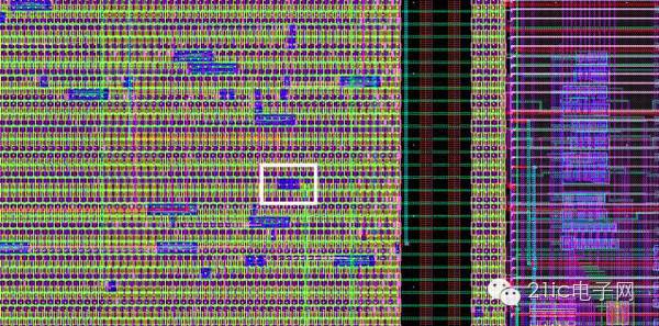
Zoom in again...
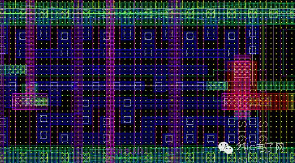
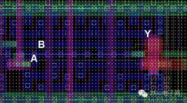
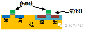
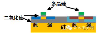
We finally see a gate! This is a NAND Gate, probably like this:
The images are arranged according to the production steps, but the steps are summarized separately.
1. **Wet wash**: Using various reagents to keep the surface of the silicon wafer free of impurities.
2. **Lithography**: Using ultraviolet light to illuminate the silicon wafer through a mask. The exposed areas will be washed away, while the unexposed areas remain. This allows the desired pattern to be engraved on the silicon wafer. At this stage, no impurities have been added yet—it's still just a silicon wafer.
3. **Ion implantation**: Adding different impurities at different positions on the silicon wafer. These impurities form the FET depending on their concentration and position.
4. **Dry etching**: Removing unwanted parts that were previously lithographically defined for ion implantation. This is done using plasma or additional lithography.
5. **Wet etching**: Further cleaning using chemical reagents.
6. **Plasma rinsing**: Bombing the entire chip with a weaker plasma beam.
7. **Heat treatment**, which includes:
- **Rapid thermal annealing**: Exposing the entire film to high-power lamps at over 1200°C, then cooling it down to activate the injected ions and perform thermal oxidation.
- **Annealing**
- **Thermal oxidation**: Creating silicon dioxide, which forms the gate of the field-effect transistor.
8. **Chemical vapor deposition (CVD)**: Further fine treatment of substances on the surface.
9. **Physical vapor deposition (PVD)**: Similar to CVD, used to add coatings to sensitive parts.
10. **Molecular Beam Epitaxy (MBE)**: Required if long single crystals are needed.
11. **Plating treatment**
12. **Chemical/mechanical surface treatment** – the chip is almost ready.
13. **Wafer testing**
14. **Wafer polishing** – and now it's ready for factory packaging.
Let’s go through the process step by step:
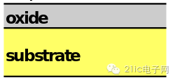
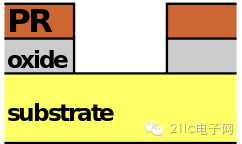
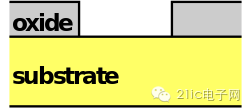
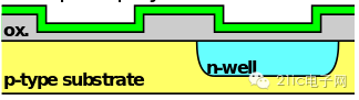
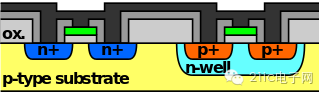
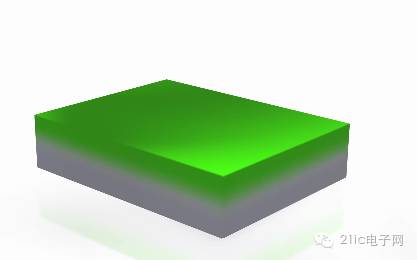
1. The top layer is the oxide, and the bottom is the substrate (silicon) — wet wash.
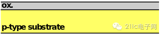
2. A small amount of P-type material is implanted into the entire substrate as the base — ion implantation.
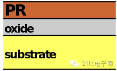

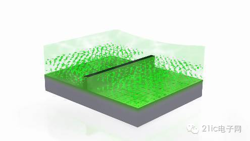
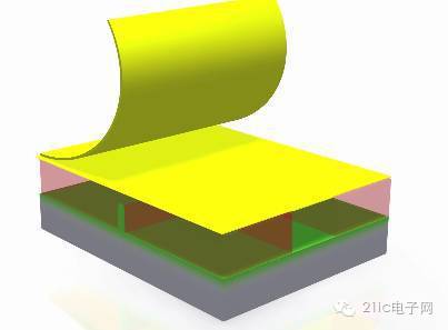
4. The upper mask! (That's where the Cr is marked. The middle empty area is not covered, and the black area is hidden.) — Lithography
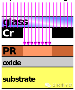
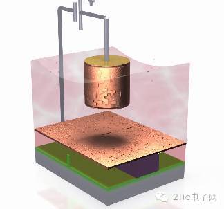
5. Ultraviolet light goes up... The following is the illuminated part — Lithography
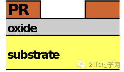
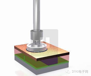
6. Remove the mask — Lithography
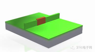
7. Wash the exposed oxide layer to expose the silicon layer (you can implant ions) — Lithography
8. Remove the protective layer. This results in a silicon wafer ready for ion implantation. This step is repeated multiple times on the silicon wafer (tens or even hundreds of times).
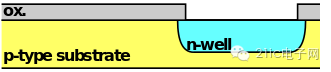
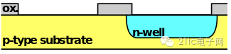
9. After lithography, insert a small amount of N-type material to create an N-well — ion implantation
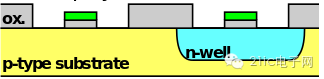
10. Dry etching is used to etch the area where the P-well is needed. It can also be etched out again using lithography — Dry etching

11. Re-oxidize a thin layer of silicon dioxide on the P-type semiconductor — Heat treatment
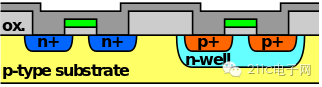
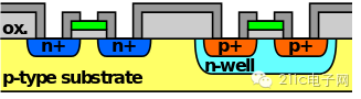
12. Use molecular beam epitaxy to treat a layer of polycrystalline silicon, which is conductive — Molecular beam epitaxy
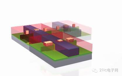
13. Further etching to make a fine structure. (In annealing and partial CVD) — Repeat 3–8 lithography + wet etching

14. Inject a large amount of P/N-type material again, and note that the MOSFET has been basically formed — Ion implantation
15. Nitride layer formed by vapor phase deposition — Chemical vapor deposition
16. Etch nitride out of the channel — Lithography + wet etching
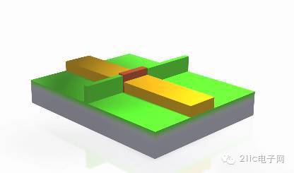
17. Physical vapor deposition of the metal layer — Physical vapor deposition

Title: *IC Fabrication Technology* By BOSE
Let’s talk about lithography. The main question is: How is lithography done for features smaller than the diameter of a hair, say 100nm?
For example, if we want to make a 100nm gate (90nm technology), it actually looks like this:

This mask is the first layer. It is made in two ways: Emulsion Mask and Metal Mask.
**Emulsion Mask:**
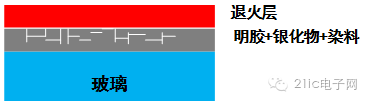
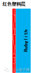
This product resolution can reach 2000 lines/mm (in fact, very bad... so sub-micron, that is, VLSI below the micrometer level doesn't need to use it). How to make it: First, you need to engrave a shape 20 times larger than the desired mask on Rubylith (not translated...) (probably 200 times the actual size of the production), this shape can be carved out with a laser, only a micron scale.

Give it! Photo! Photo! The photo is Emulsion Mask! Give it! Photo! Photo! Emulsion Mask! If the photo to be taken is too large, there is also a method of sub-area.
**Metal Mask:**

Production process:
1. Make an Emulsion Mask first, then use the Emulsion Mask and the 17-18 steps I mentioned before to make the Metal Mask! There is a feeling of recursion in the moment!
2. Electron beam: Probably long like this
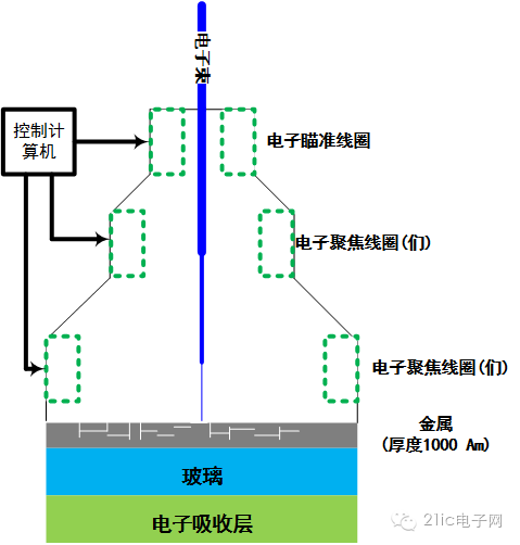
Just like the printer, just hit it underneath. The advantage is that the accuracy is particularly high. Most of the high-precision (<100nm technology) uses this mask. The disadvantage is too slow...
After making a mask:
Feature Size = k * λ / NA
Where k is generally 0.4, related to the production process; λ is the wavelength of the light used; NA is the magnification of the lens as seen from the chip.
At the current state of the art, this formula has changed because as the Feature Size decreases, the thickness of the lens becomes a problem.
Feature Size = k * λ / NA²
Well, in fact, the mask can be made larger than the chip. As for the specific production method, it is usually directly carved with a high-precision computer probe + laser. Photomask (mask) material selection is generally more flexible than silicon wafer, can be made from materials that are easily vaporized by laser.
This lithography method is a black technology general point! Directly reduce λ by an order of magnitude, with no extra cost! You say no!
Food for Thought: Wikipedia’s layout on the mask gives such a picture. What kind of shape would it be made with such a mask?
The steps of the drawing are labeled below each figure for a total of 18 steps.
The final shape is probably as long as this:
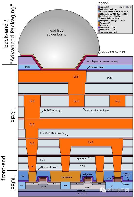
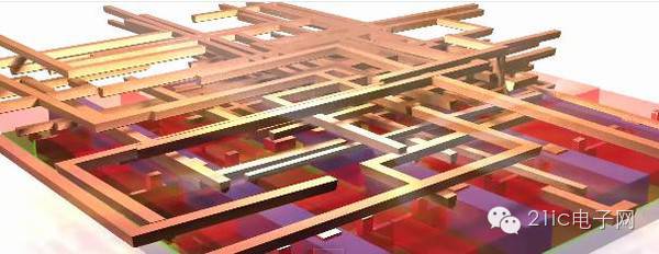
Among them, steps 1–15 belong to the front-end processing (FEOL), that is, how to make the FET.
Steps 16–18 (plus a lot of repetitions) belong to the back-end processing (BEOL), the back-end processing is mainly used for wiring. The basics that can be seen in the big chip at the beginning are all wiring! Generally, a highly concentrated underlying silicon chip is almost invisible on the chip and will be blocked by the wiring.
**SOI (Silicon-on-Insulator) technology:**
The drawbacks of traditional CMOS technology are: The thickness of the substrate affects the parasitic capacitance on the chip, which indirectly leads to the performance degradation of the chip. The SOI technology mainly separates the source/drain and the silicon substrate to achieve (partially) eliminate parasitic capacitance.
Tradition:
There are mainly the following methods (mainly in the fabrication of silicon-silicon dioxide-silicon structure, the subsequent steps are basically the same as the traditional process.)
1. High temperature oxidation annealing:
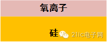
Oxygen ions penetrate into the silicon layer to form an oxygen-rich layer.
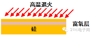
forming.
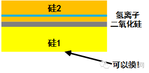
Or 2. Wafer Bonding (with two pieces!) Isn't it the same structure as a sandwich cookie? Yeah, it's not bad! Come two!
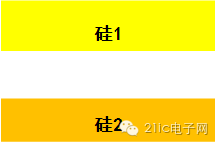
Come two!
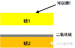
Surface oxidation of silicon 2

Hydrogen ion implantation of silicon 2 and hydrogen ion implantation of silicon 2
Turn over
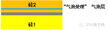
Treating the hydrogen ion layer into a bubble layer and treating the hydrogen ion layer into a bubble layer
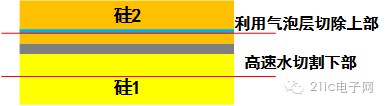
Cut off the excess and cut off the excess
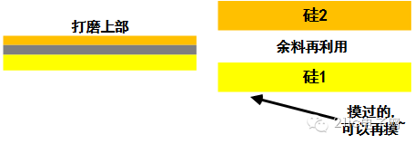
Molding! + Reuse

Lithography

The micrograph is as long as this:
Photolithography + etching

Remove the protection, the middle one is Fin to remove the protection, the middle one is Fin
Polysilicon/high-k dielectric growth of polysilicon/high-k dielectric gates at the gate
Oxide layer growth at the gate of the oxide layer in the gate

Growing into this

Source drain fabrication (lithography + ion implantation)
Primary metal/polysilicon patch

Etching + molding
The physical vapor phase grows out of the surface metal layer (because it is a three-dimensional structure, all the wires are connected at the top)
Mechanical grinding (right! Ungrinding will result in inconsistent metal layer thickness)
Molding! Forming!
Probably the sauce purple...
Pocket Type Nickel Cadmium Battery
The nickel–cadmium battery (NiCd battery or NiCad battery) is a type of rechargeable battery using nickel oxide hydroxide and metallic cadmium as electrodes. The abbreviation NiCd is derived from the chemical symbols of nickel (Ni) and cadmium (Cd).
Pocket Type Nickel Cadmium Battery capacity range is from 10ah to 1200ah, have three series: low discharge rate, medium discharge rate and high discharge rate.
Nickel Cadmium Batterie,Nicd Battery Pocket Plate,Railway Nicd Battery,10~1200Ah Nicd Battery
Henan Xintaihang Power Source Co.,Ltd , https://www.taihangbattery.com