The importance of power integrity and signal integrity in board design is self-evident. This article briefly introduces the simulation of power integrity. After obtaining the impedance curve of the power supply, how to set the decoupling capacitor to reduce its overall operation. The impedance in the frequency band, thereby achieving the purpose of reducing EMI.
First, we choose a board. The layout is company, so it's blackened here, probably knowing it's a board.

We choose a 5V USB cable, the power is fed from the upper right corner, and after passing 4 capacitors in the lower left corner, it reaches the USB interface.

According to the USB standard, the current USB3.0 transmission speed is affected by the hard disk, and the maximum is no more than 1 Gbps. Therefore, we pay attention to the frequency of 100 kHz to 2 GHz, which is set as the simulation frequency band because the Net trace is not long. There is no snake-shaped curved part, so it is predicted that the impedance change is not very large. In order to save the boss cost, three capacitors are directly selected here. First, get the spice model of the simulation object.
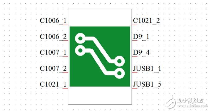
D9_1 and JUSB1_1 are feed and feed respectively, and the corresponding D9_4 and JUSB1_5 are GND pins. Set the internal resistance of the power supply to 0.1Ω, and then connect the circuit. The position of the three capacitors is empty first. Check the impedance characteristics of this Net.
After the simulation is finished, the impedance parameter map of the power supply trace is obtained as follows:

It can be seen that since the USB trace is relatively short and the wiring is relatively standardized, the impedance does not change much in the 2 GHz range, and the maximum is 391 Ω. There are several obvious resonances in the power signal in this frequency band. In order to reduce EMI, decoupling capacitors need to be added. The goal is to reduce its impedance across the entire frequency band to less than 10 Ω.

Next, connect the three capacitors, which are C1, C2, and C3. The initial capacitance is set to 1000pf, and three resistors are connected in series, which are R1, R2, and R3. Optimization goal: 100kHz-2GHz impedance is less than 10Ω.

The result after optimization:
C1 = 3111.65
C2 = 3122.21
C3 = 3111.49
R1 = 7.14841
R2 = 16.6401
R3 = 40.4783

The figure above shows the Z1_1 curve for port 1, the green curve is the optimized result, and the red is the initial result. Using 3 capacitors feels that the target has not yet been reached, but from the flatness of the waveform, it is indeed much better than the beginning.
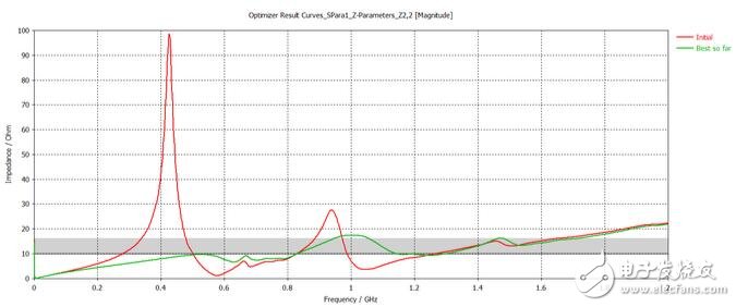
The figure above shows the Z2_2 curve of port No. 2. The green color is the optimized result, which basically meets the requirements, and the flatness of the waveform is very good.
In summary, the layout board diagram should take into account power integrity, signal integrity, and EMC issues during the initial design process, which eliminates the need for subsequent extensive testing, rectification, and modification of board diagrams and process time and costs.
This article is reproduced in electromagnetic compatibility (EMC) public number, author: gravy; Reprinted with permission from the author and indicate the source, thank you.
130 Watt Solar Panel,Solar Panel Kits,100W Polysilicon Solar Panel,130W Polysilicon Solar Panel
Zhejiang G&P New Energy Technology Co.,Ltd , https://www.solarpanelgp.com