Radio frequency reader based on FM1702SL
system design
The system block diagram is shown in Figure 1. The system consists of MCU, keyboard, EEPROM, FMl702SL, LCD screen, and 485 communication module. MCu controls FMl702 to read and write the Mifare card, and then performs corresponding operations on the LCD screen and EEPROM according to the corresponding data obtained. The MCU communicates with the PC through the 485 bus. Even if the communication between the PC and the MCU is abnormal, the MCU can work independently. After the communication with the PC is restored, the MCU can transfer the information backed up in the EEPROM to the PC.
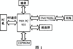
P8912C931 is a single-chip package microcontroller. P89LPC931 uses a high-performance processor structure, instruction execution time only needs 2 to 4 clock cycles. P89LPC931 integrates many system-level functions, which can greatly reduce the number of components and Circuit Board area, and reduce the cost of the system. The EEPROM uses FM24C64L, which is a memory chip with I2C as the operation mode. The LCD driver chip is PCF8576, which also uses I2C as the operating mode. The entire system is powered by a 12V power supply, which is then regulated by a voltage regulator chip 2576 to 3.6V.
working principle
The Mifare card contains an EEPROM with a capacity of 8K bits, 16 sectors, each sector is 4 blocks, each block is 16 bytes, and each block has an independent set of passwords and access. control. Each card has a unique serial number, which is 32 digits. No power supply, built-in high-frequency antenna, contains encryption control logic and communication logic circuit.
The information is stored in the Mifare card, and the reader and the Mifare card establish a non-contact information transmission channel between the two through their respective antennas. When the Mifare card enters the work area of ​​the human system, the reader sends a set of fixed frequency electromagnetic waves to the Mifare card. The Mifare card has an LC series resonance circuit whose frequency is the same as the frequency emitted by the reader. The Lc resonant circuit resonates, so that there is a charge in the capacitor. At the other end of the capacitor, a unidirectional electronic pump is connected to send the charge in the capacitor to another capacitor for storage. When the accumulated charge When it reaches 2V, this capacitor can be used as a power supply to provide working voltage for other circuits, transmit the data in the card or read the data of the reader. The maximum communication distance can be changed by adjusting the antenna drive voltage.
Interface circuit between FMl702SL and MCU
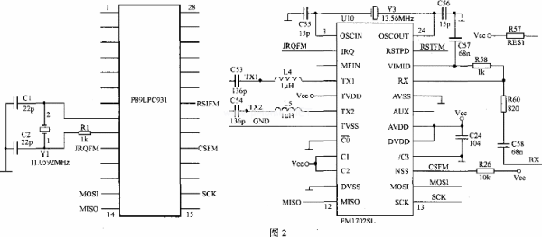
The circuit is shown as in Fig. 2, MCU and FMl702SL communicate through SPI bus line, adopt the work mode of cutting off. It should be noted that after the FMl702SL is reset, an initialization procedure must be performed to initialize the SPI interface mode, and the startup work of the MCU and FMl702SL can be synchronized.
Design of reader antenna
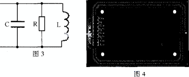
According to the principle of mutual inductance, the larger the radius and the more the number of turns, the greater the mutual inductance coefficient of the antenna on the reader and the antenna on the card. According to the requirements of international standards, the communication distance between the card and the reader is 10cm. The antenna can be equivalent to a parallel circuit of R, L, and c. The schematic diagram is shown in Figure 3. In Figure 3, L is the self-inductance of the antenna, R is the equivalent resistance of the antenna, and C is the distributed capacitance of the antenna. Figure 4 shows the PCB of the antenna.
Pay attention to the quality factor of the antenna when designing the antenna. The international standard ISOl4443 stipulates that regardless of the TYPEA or TYPEB contactless IC card, the data transmission speed between the reader and the card is 106kbit / s, the carrier frequency f0 = 13.56MHz, therefore, the time for each bit of data to maintain tO = 106 ï¼ 104k = 9.44μs, the signal encoding of the TypeA RF card smart card reader to the RF card is a modified Miller encoding, and the transmission of each digit has a carrier interruption of t = 3μs, so the bandwidth of the signal is approximately B = "lT" = 1 / 3μs = 333.333kHz, so the quality factor of the antenna Q = fO / B = 13.56 MHz33.333kHz = 35, the transmission bandwidth of the antenna is inversely proportional to the quality factor. Therefore, an excessively high quality factor will cause the bandwidth to shrink, thereby weakening the modulation sideband of the reader, which will cause the reader to fail to communicate with the card.
The operation process of the reader on the card
There are 8 register pages inside FMl702SL, each page has 8 registers, and each register has 8 bits of data. These registers are unified addressing, from Ox00 ~ 0x3F, MCU communicates with FMl702SL through SPI interface to set up these registers. For example, when the MCU needs FMl702SL to execute a command (Transceive), write the command code (1E) to the Command register.
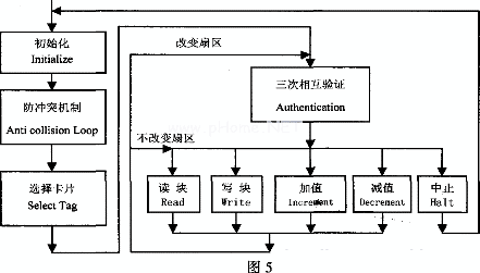
It must be noted that the operation of the MCU on the card is not a simple instruction can be completed, which must have the FMl702SL hardware internal register settings. The operation steps are shown in Figure 5.
(1) Reset and initialize FMr702SL: initialize the SPI interface of FMl702SL, initialize the FMl702SL timer, set the timer control register, and open Txl and TX2.
(2) Request: When a Mifare card is within the working range of the antenna of the card reader, the programmer controls the reader to issue the R: EQUEsT all (or REQUEsT std) command to the card. The ATR of the card will be activated, and a total of 2 bytes of the card type (TagType) number in the card BLOCkO will be transmitted to the reader, and the first step of communication between the card and the reader will be established. If the reset request operation is not performed, other operations on the card by the reader will not be performed.
(3) AnTIeollision LOOp (anti-collision mechanism): If there are multiple Mifare cards within the working range of the antenna of the card reader, the reader will first communicate with each card to obtain each card Serial number. Since each Mifare card has its unique serial number, it will never be the same, so the reader will ensure that only one card is operated at a time according to the serial number of the card. The card reader's return value is the serial number of the card.
(4) Select Tag: After completing the above two steps, the reader must select the card. After performing the operation, return the SIZE byte on the card.
(5) AuthenTIcaTIon (three mutual authentication): After the above three steps, when confirming that a card has been selected, the reader must authenticate the password that has been set on the card before reading and writing the card. If they match, further read and write operations are allowed.
(6) Read and write operations: The final operations on the card are operations such as reading, writing, adding value, decreasing value, storing and transferring.
Flash Gold+Hard Gold board. the base Material is FR4 IT180A (TG180). 8-layer PCB.Copper thickness is 1oz inner-layer/1.5oz outer-layer.Board Thickness is 1.8mm and the Min.Hole Size is 0.3mm. Min.Line Width/Min.Line Spacing is 0.25mm/0.25mm. green solder-resist & white silkscreen. E-test: 100%. Flash Gold(hard Gold) is an expensive surface treatment, which has the advantage of being able to withstand friction.
")
Flash Gold(hard Gold)
Flash Gold,Custom Flash Gold,Hard Gold,Stick Flash Gold
Orilind Limited Company , https://www.orilind.com