Abstract: A 5.8GHz microwave receiver circuit design scheme is proposed. In accordance with the requirements given by the system standard, the principles and methods of receiver system design are proposed, the specific circuit design is introduced, and the experimental results and analysis are given.
DSRC, as a dedicated wireless short-range communication protocol, is mainly aimed at the communication interface specification between the roadside unit (RSU) fixed on the lane or roadside and the onboard unit (OBU) reproduced on the mobile vehicle. This article uses the widely used passive European DSRC standard. Its main technical indicators are as follows: the operating frequency is 5.8 GHz, the downlink data is FMO coding, the rate is 500 kbps, and the modulation method is amplitude (AM) modulation; the uplink data is NnZI coding, the rate 250kbps, the modulation mode is 2MHz or 1.5MHz subcarrier binary phase shift keying (BP5K) modulation, and the data error rate is 10-6. Figure 1 shows the working mode of the DSRC communication system. It uses half-duplex communication mode, there are two main working methods: downlink and uplink. When in the downlink mode, RSU is in the transmission mode, and OBU is in the reception mode, and the RSU transmission adds the modulation signal F AM to the carrier frequency F0 of 5.8 GHz in the AM modulation mode. When in the uplink mode, RSU is in receive mode, while OBU is in transmit mode, and RSU transmits continuous j. The SCHz carrier FO is given to the OBU and mixed with the 2MHz or 1.5MHz subcarrier BP5K modulation signal Fm in the OBU, and then reflected back to the receiver on the R5U through the antenna for synchronous demodulation.
This paper proposes a set of 5.8GHz microwave receiver circuit with OBU and RSU for the given requirements of the DSRC communication system. It has the characteristics of high sensitivity and large dynamic range. At the end, the experimental conditions of the system are introduced.
figure 1
1 Design principle
1.1 The range and sensitivity estimation of the receiving system
The OBU's downlink wake-up action distance is:
(1) In the formula, λ = wavelength of the carrier = 5cm; po = power output of the RSU transmitter = 18dBm; Gt is the antenna gain of the RSU: 13dB; Gr = OBU antenna gain = 6dB; Ls = caused by the vehicle windshield Loss = -5dB; Smin = OBU's wake-up sensitivity = -40dBm. Therefore, the downlink wake-up action distance of OBU can be obtained at about 15m.
The power received by OBU is modulated by OBU's BP5K subcarrier and then transmitted back to the RSU receiver. Therefore, the received power is:

(2) In the formula, Lb is the subcarrier modulation and forwarding loss of the OBU, which is about -6dB; the month is the distance between the OBU and the RSU receiver in the uplink. Therefore, when the normal communication range is only 5m-1lm, the dynamic fluctuation of the RF end of the R5U receiver is -84dBm ~ -97dBm, and the sensitivity of the RSU receiver must be <-97dBm.
1.2 Overall design of RSU receiver
This system is a microwave reflection type system, and the carrier wave of the RSU transmitter reflected by the OBU is used as the uplink transmission carrier wave, so the RF signal of the RSU receiver is the same as the local oscillator 10 signal. Therefore, this receiver is designed with a zero-IF receiving scheme. Because the upstream subcarrier BPSK modulation signal is a double-sideband modulation, its spectrum is located on both sides of the carrier frequency, so no image frequency suppression is required. As shown in Figure 2, the RSU receiver is mainly composed of a radio frequency band-pass filter, a low-noise amplifier, a frequency converter, an intermediate-band pass filter, and an intermediate-frequency amplification and BPSK demodulation circuit.
figure 2
According to the requirements of the system on the receiver, the receiver design mainly focuses on the following aspects: receiver noise figure design, receiver large dynamic range design, and receiver microwave passive component accurate design. Considering its comprehensive performance, in the specific circuit design, it is necessary to design the noise figure and power gain of all levels in a balanced manner, to ensure the accuracy of each passive component, and to reasonably allocate the indicators of some circuits to meet the system requirements for the receiver.
1.3 Sensitivity of RSU receiver
The bit error rate BER of the coherent demodulated BPSK signal is:
(3) In the formula, S / N is the signal-to-noise ratio of the input signal. Therefore, in order to obtain a data error rate of 10-6 or less, the signal-to-noise ratio at the intermediate frequency amplifier end must be greater than 10.5 dB. The signal power required by the RSU receiver can be expressed as:
PUR = 10lg (kT) + 10lgB + NF + S / N (4)
(4) In the formula, k = Boltzmann's constant, T = room temperature (290K), B = intermediate frequency bandwidth = 1 MHz, NF = noise coefficient of the front end of the intermediate frequency amplifier of RSU, and S / N is the signal-to-noise ratio of the input end of the intermediate frequency amplifier> 10.5dB.
The noise figure of the front end of the RSU IF amplifier is:

(5) In the formula, NF1 = 1 / G1 = RF bandpass filter insertion loss = 2dB, NF2 = low noise amplifier noise figure = 2.1dB, NF3 = mixer unilateral noise figure = 5dB, G2 = low noise amplifier Gain = 24dB (see Figure 2). G3 = Gain of the mixer = -8dB, NF4 = Noise factor of the mid-band pass filter = 3dB.
When S / N is the minimum required signal-to-noise ratio (10.5dB), the sensitivity of the RSU receiver can be obtained as:
Pmin = (-114 + 4.2 + 10.5) dBm≈-99dBm <-97dBm
Therefore, it can meet the design requirements of the system.
1.4 The dynamic range of the RSU receiver
Dynamic range refers to the ratio of a strong out-of-band signal level to a very weak signal that reduces receiver performance in some way. The weak signal usually considered is the receiving sensitivity. The dynamic range is usually expressed in two ways, namely, the single-tone dynamic range expressed by IdB gain compression and the two-tone dynamic range expressed by third-order intermodulation. In this receiving system, the single tone dynamic range is mainly considered. The total third-order intermodulation input intercept point (IP3) 3 of the RSU receiver is:
(6) In the formula, (IP3) 1 = I / P of the RF band-pass filter = ∞, (IP3) 2 = IP3 of the first-stage LNA = 15dBm, (IP3) 3 = IP3 of the second-stage LNA = 23dBm ; (IP3) 4 = IP3 of the mixer = 14dBm; Gi is the gain of the above stages, of which G2 = 15dB, G3 = 9dB, two stages total 24dB, other gain values ​​shown in Figure 2. Therefore, we can obtain:
 ,
,
Get (ï¼ P3) o = -8dBm.
Generally speaking, the IldB input compression point Pldb-in is about 10dB lower than the third-order intermodulation cutoff point, so the total Pldb-in of the RSU receiver is about -18dBm, so the dynamic range of the receiving end is -99dBm--18dBm. During normal communication of this system, the working signal range of the receiving end is -97dBm--84dBm, but because the output power of the transmitter is 18dBm, and the isolation between the receiving and transmitting antennas is> 38dB, considering the strong signal coupling of the transmission, the receiver receives The maximum signal Pmax = (18-38) dBm = -20dBm. Therefore, the dynamic range of the actual received RF signal terminal is -97dBm ~ -20dBm. Obviously, the dynamic range of the RSU receiver meets the requirements of the system.
1.5 Design, simulation and production of microwave components of RSU receiver
The radio frequency band-pass filter adopts a three-stage cascading method of coupled microstrip lines. The structure is compact, the center frequency of the parasitic pass band is higher, and the applicable frequency band range is large. Figure 3 shows the S21 and S11 parameters of the band-pass filter simulation. The band-pass filter 3dB bandwidth is 5.65GHz to 5.95GHz, and the attenuation is> 20dB at the out-of-band frequency points of 5.3GHz and 6.3GHz. The actual tested in-band insertion loss S21 is 1 ~ 2dB larger than the simulated design. This is because the relative frequency band of the filter is only about 4%. At this time, the radiation loss of the coupling line has a large influence on the Q value, resulting in increased in-band attenuation. .
image 3
The fan-shaped line is used in the DC bias circuit of the microwave active device. It together with the DC blocking capacitor ensures the isolation of the DC bias from the RF signal. The length of the sector and the length of the connection are about 1/4 wavelength of the center frequency. The connection is generally made in a curved form to facilitate fine-tuning of its length. The included angle is 45 degrees. It shows that the sector-shaped partial line is in the frequency band of 5.7GHz ~ 5.9GHz, the insertion loss is less than 0.5dB, and its return loss is about 40dB, so it can isolate the RF signal better.
2 Receiver circuit design technology
2. 1 OBU circuit design
The block diagram of the OBU circuit is shown in Figure 5. SB_out is the maximum signal for wake-up DC output, DATA_out is the demodulated downstream FMO code output, and MOD is the downstream 2MHz carrier BPSK modulated signal input terminal. This working mode is selected and controlled by WK in and T / R. The wake-up sensitivity of OBU is about -40dBm, and the forwarding loss is about -6dB. When making PCBs, pay attention to the peripheral devices as close as possible to the IC and the wiring as short as possible to reduce the influence of the distribution parameters. Connect a 1/4 wavelength short wire to the ground at the RF port to protect the OBU from damage caused by static electricity or other transient interference.
Figure 4
2. 2 low noise amplifier circuit of RSU receiver
In order to better achieve the balance of noise and gain, this system uses two stages of low noise amplification. The idb compression point is small, the noise figure is small and the gain is large as the pre-amplification. Pay attention to the anti-static protection and electromagnetic shielding of low-noise Cao to prevent its oscillation from affecting performance.
2. 3 RSU receiver mixer circuit design
Generally speaking, the performance of passive balanced mixer is the best, it has higher second-order and third-order intercept points, and has better noise balance performance, but the disadvantage is that it requires a large local oscillator power and has a large Frequency conversion loss. The passive double-balanced mixer MMIC is used here. When the RF signal frequency is 5.8 GHz and the LO input power is 10 dBm, the conversion loss is 8 dB, the bilateral noise figure is 5 dB (the bilateral band is 8 dB), and the input is 1 dB. The compression point is 9 dBm, the third-order intermodulation cutoff input point is 14 dBm, the LO-RF signal isolation is 30 dB, and the LO-IF isolation is 25 dB. 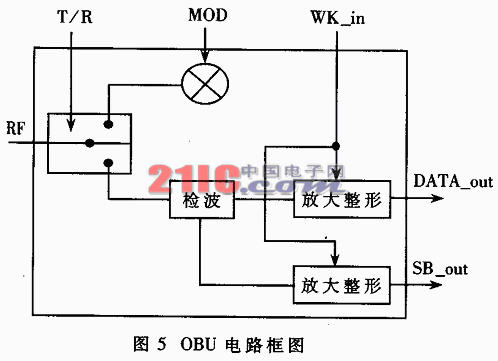
2. 4 RSU receiver intermediate frequency filter / amplifier circuit
The frequency characteristics of the intermediate frequency system, such as center frequency, pass band, in-band fluctuations, and out-of-band attenuation, mainly depend on the intermediate frequency filter, which is usually an LC filter. Here, a low-pass-high-pass band-pass filter is used. The spectrum of the BPSK signal is similar to the double-sided band of carrier suppression, and its bandwidth is twice that of the baseband signal, that is, 500 kHz. However, considering 2MHz or 1.5MHz as the carrier center frequency, the filter center frequency is 1.75MHz, the 3dB bandwidth is 1MHz, and the out-of-band rejection is greater than 30dB at 0.3MHz. DC low frequency signal is greater than 35dB at 10MHz to prevent interference from out-of-band signals.
The intermediate frequency amplifier consists of four stages. The first three stages are bipolar amplifier MMICs with low noise figure and wide band operating range, and the final stage is a video broadband op amp. The four-stage gain is about 7 & lB. Because the gain is high, it is easy to cause positive feedback to generate self-excitation, and a stable resistance can be connected in parallel between stages to ground, generally about 100 ohms.
2. 5th SU receiver system index test
The RSU receiver system index measurement scheme is as follows: the receiver local oscillator input frequency is 5797. 5MHz, the power is 10dBm frequency source, the network analyzer HP8753ET output is connected to the receiver signal after attenuation by the attenuator, and the HP8753ET output frequency is 5799.5MHz single frequency continuous wave, the power can be adjusted, use the spectrum analyzer to test the output power value at the frequency of 2MHz. The test results are shown in Table 1.
Table 1 Experimental test results
| Signal input power (dBm) | Body noise (without input) | -102 | -97 | -92 | -88 | -86 | -84 | -82 |
| Corresponding power value (dBm) | -twenty one | -13 | -9 | -4 | 0 | 2 | 4 | 4 |
It can be seen from Table 1 that the actual body noise is about 2dB larger than the design. At -97dBm, the signal-to-noise ratio S / N of the output signal is 11dB. When the input power at the signal end of the receiver is -82dBm, clipped distortion occurs. However, when the input power of the receiver signal end is -97dBm · -84dBm, the gain is + 87dB, which is basically linearly amplified to meet the system requirements.
This paper presents a set of 5.8GHz microwave receiver circuit, and gives the experimental results. It can be applied to highway wireless non-stop toll collection system based on DSRC or other wireless communication system with working frequency of 5.8GHz.
Double Socket Extension,Stainless Steel Wall Sockets,Gang Socket Extension,Zebronics Power Extension Socket
Heikki Technology Co., Ltd. , https://www.heikkipower.com