Since the voltage amplitude of the CCD driver is reduced, the power consumption of the CCD driver is greatly reduced. Since the differential mode inductance of the common mode choke is small, the resonance of the capacitive load of the CCD is effectively avoided, so the scheme can ensure the quality of the driving signal. The board was designed and tested for the circuit designed by the solution. The experimental results show that the circuit designed in this scheme can effectively reduce the power consumption of the driver circuit under the premise of ensuring the quality of the driving signal.
0 Preface
Charge-coupled device (CCD) has been widely used in the field of optoelectronic imaging. It has the advantages of high speed, low noise, wide dynamic range and linear response. However, for the CCD to work properly, imaging circuit support is needed. Among them, the CCD driving circuit is an important part of the imaging circuit, and the driving circuit is responsible for moving the charge packets collected by the CCD through the shift register to the output node for outputting the signal voltage. Since it is a serial shift, a high-speed drive circuit is required, and in the field of high-speed imaging, the drive circuit operates at a higher speed. In addition, the voltage amplitude of the CCD driving waveform is often very high, and the shift register of the CCD is a capacitive load. The high-speed large-voltage amplitude driving the capacitive load requires a large power consumption. Therefore, the power consumption of the CCD-based imaging system is relatively high. Large, power consumption leads to higher CCD driver temperatures, which can affect system reliability and lifetime.
To solve this problem, the CCD driver is used to first generate a low-voltage driving signal, and then use a common-mode choke to amplify the voltage. Since the voltage of the CCD driver is lowered, the power consumption of the CCD driver itself is drastically reduced. Since the differential mode inductance of the common mode choke is small, it can effectively avoid resonance with the capacitive load of the CCD, so the quality of the driving signal can be ensured.
1 CCD drive circuit analysis
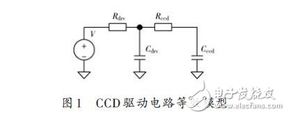
In order to design a high-speed low-power CCD drive circuit, the CCD drive circuit is first modeled and analyzed. Figure 1 shows the equivalent model of the CCD drive circuit. Where V is the signal output of the driver, Rdrv represents the Thevenin equivalent internal resistance of the driver, Cdrv represents the equivalent capacitance of the driver, Rccd represents the equivalent series resistance of the trace inside the CCD, and Cccd represents the equivalent load capacitance of the CCD. It can be seen that the CCD driving circuit is an RC charging and discharging circuit.
For RC circuits, the power dissipation can be approximated by equation (1).
Where: C is the capacitance value; V is the signal voltage amplitude; f is the signal operating frequency. The term of resistor R is not included in the equation, but the actual power dissipation is consumed on resistor R because the capacitor does not consume power. For the same capacitor C, when the resistance value R is large, the transient current value is small but the transient current duration is longer; when the resistance value R is smaller, the transient current value is larger but the transient current duration is shorter. . This is why there is no resistance R term in the formula.
Equation (1) also indicates that the power dissipation is proportional to the square of the voltage. Therefore, as long as the voltage amplitude is reduced, the power consumption can be greatly reduced. The driving voltage of the CCD is often very high. For example, the reset pulse driving voltage amplitude of many CCDs can reach 10 V. The power consumption of the driving circuit is composed of the power consumption of the driver and the power consumption of the CCD. The power consumption of the driver is due to the parasitic capacitance inside the driver. For example, the internal capacitance of the CCD driver EL7457 is about 80 pF. The voltage amplification through the common mode choke can reduce the output voltage amplitude of the driver, which can effectively reduce the power consumption of the driver.
Black Light Tube,Blb Tube,Blb Bulb,Blb Lamp
Changxing leboom lighting product CO.Ltd. , https://www.leboomuv.com