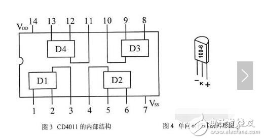
The CD4011 integrated circuit is a CMOS device that contains four independent NAND gates. Each gate has two inputs and one output. The output of a NAND gate is low (0) when both inputs are high (1), and it becomes high (1) in all other cases. This makes the CD4011 a versatile component for digital logic circuits.
This article discusses a sound and light controlled delay switch circuit built using the CD4011. It provides a detailed explanation of how the circuit works, including component selection, assembly, testing, and troubleshooting. Let's take a closer look at each part of the process.
**First, the working principle of the circuit**
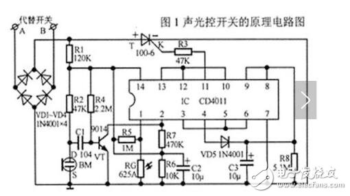
The schematic diagram of the sound and light controlled delay switch is shown in Figure 1. The main component in this circuit is the CD4011, which contains four NAND gates (VD1 to VD4). These gates help keep the circuit simple and reliable.
As its name suggests, the sound and light control delay switch turns on the lights when it detects sound, such as footsteps or clapping, and then automatically turns them off after a short delay. The overall function of the circuit is to activate an electronic switch based on sound input. Once the signal path is clear, the circuit can be divided into functional blocks, as shown in Figure 2.
Figure 1 and Figure 2 together explain how the circuit operates. The sound signal, such as a footstep or clap, is captured by an electret microphone (BM) and converted into an electrical signal. This signal is then amplified by transistor VT through coupling capacitor C1. The amplified signal is sent to the second pin of NAND gate VD1. R4 and R7 are bias resistors for VT, while C2 serves as a power supply filter.
To ensure the circuit only activates during nighttime, a light control circuit is used, consisting of a photoresistor (RG) and other components. When it's dark, the resistance of RG increases, resulting in a higher voltage across it. This voltage is used to trigger the delay mechanism, which involves resistor R8 and capacitor C3. The time constant t = 2Ï€R8C3 determines the length of the delay. Adjusting R8 or C3 allows the delay time to be customized for different applications.
VD3 and VD4 form a two-stage shaping circuit that processes the square wave signal. When C3 charges to a certain level, the output from the NAND gates goes high, triggering the unidirectional thyristor and turning on the electronic switch. When C3 discharges, the output from the NAND gates drops to low, causing the thyristor to turn off and the switch to close.
Diodes VD1 to VD4 also serve to rectify the AC 220V supply, converting it into pulsating DC power. Resistor R1 steps down the voltage, and C2 filters the power to provide a stable DC supply for the microphone, transistor, and IC.
**Schematic:**
**Board diagram:**

This type of delay switch is ideal for replacing traditional switches in residential corridors. It ensures that lights turn on automatically when someone walks through, providing illumination for a few minutes before turning off. During the day, even if there is noise, the lights will not turn on, saving energy. This circuit is also suitable for use in public places like factories, office buildings, and schools.
It offers advantages such as compact size, aesthetic design, ease of construction, and reliable performance, making it a great project for electronics enthusiasts.
**Second, component selection**
The CD4011 is chosen as the main IC, containing four independent NAND gates. The thyristor T is a 1A/400V unidirectional thyristor (model 100-6). For larger loads, higher current thyristors like 3A, 6A, or 10A can be used. The electret microphone is selected from a standard recorder. The photoresistor is of type 625A, with a resistance of 20kΩ in bright light and over 100MΩ in darkness. Rectifier diodes like 1N4001–1N4007 are used. Component values can be adjusted within reasonable ranges depending on the application.
**Third, installation and production**
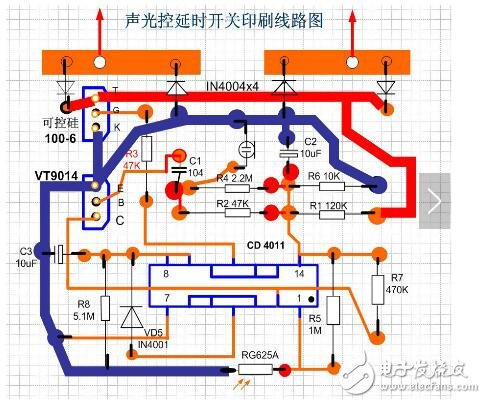
After gathering all components, use a multimeter to check their quality. During soldering, start with non-polar components like resistors and capacitors, placing them horizontally or vertically as needed. Polar components such as electrolytic capacitors, microphones, and thyristors must be installed with correct polarity to avoid damage. The PCB layout is shown in Figure 5.
**Fourth, debugging**
Before powering on, carefully check the board against the schematic to avoid errors like wrong soldering or short circuits. Avoid touching any parts of the board while powered on. Use a multimeter to test voltages at key points.
During testing, block the photoresistor and tap the microphone. If the light turns on, the circuit is functioning correctly. If not, check for faulty connections or incorrect component placement.
**Fifth, fault detection and maintenance**
Common issues include:
1. No light at night despite sound — may be due to low sensitivity. Check microphone, C1, or transistor settings.
2. Lights trigger too easily — adjust sensitivity by changing resistor values.
3. Lights come on during the day — check photoresistor placement and resistance.
4. No response to sound at night — verify input signals and check IC functionality.
5. Lights stay on constantly — may indicate a damaged thyristor.
6. Incorrect delay time — adjust R8 or C3 to change the timing.
By following these steps, you can successfully build and maintain a reliable sound and light controlled delay switch.
Infrared Optical,Zinc Selenide Lens,Optical Zinc Selenide Lens,Optical Imaging Lens
Danyang Horse Optical Co., Ltd , https://www.dyhorseoptical.com