**Foreword**
With the rapid advancement of computer technology, the USB interface has become one of the most essential external device expansion interfaces in personal computers. As a result, writing firmware for USB peripherals is a crucial step during their development. This article presents a firmware program developed using the C language within the Keil C51 software environment. The focus is on explaining the main functions, flow, structure, and endpoint configuration of the firmware. Detailed procedures for key sections are also provided. The design emphasizes simplicity, ease of modification, and testing, enhancing code readability while ensuring the program's versatility and portability.
When designing and developing a USB peripheral, developers typically need to write three key components: firmware, USB drivers, and client applications. Upon connecting the device to the host (via a USB cable), the host system detects the new device and establishes a connection. One of the primary goals of firmware development is to ensure that the operating system, such as Windows, can detect and identify the connected device. Firmware can be written in C using the Keil C51 environment, which is a powerful development tool designed for 8051 microcontrollers. It offers a wide range of library functions, integrated development and debugging tools, and a user-friendly Windows interface. Additionally, the object code generated by Keil C51 is highly efficient, with compact and easy-to-understand assembly code. For these reasons, this article focuses on using Keil C51 to develop the firmware for the PDIUSBD12 chip.
**1 Main Work Done by the Firmware Program**
The primary goal of the firmware is to enable communication between the host and the device, allowing data transfer and command execution. This ensures that the PDIUSBD12 achieves maximum transfer speed over USB. The firmware is closely tied to hardware, involving tasks such as USB device connection, protocol handling, and interrupt management. When the PDIUSBD12 receives a packet from the USB, it triggers an interrupt to the CPU. The CPU then responds by entering the Interrupt Service Routine (ISR), where it reads the incoming data, stores it in a buffer, and sets an event flag. Afterward, the CPU resumes its foreground task, checks the event flag, and performs the corresponding action.
USB microcontroller firmware is generally divided into three parts: initialization of the microcontroller and peripherals, a main loop that can be interrupted, and the interrupt service routine itself. According to the USB protocol, all transfers start from the host, so the microcontroller acts as the foreground process, waiting for interrupts. The host sends a token packet to the device (PDIUSBD12), which then generates an interrupt. The microcontroller enters the ISR, reads the interrupt register, identifies the type of token packet, and performs the necessary actions. Therefore, the core of the firmware lies in writing the interrupt service routines to handle various token packets.
Communication between the MCU and PDIUSBD12 is mainly achieved through commands sent by the MCU. These commands are categorized into initialization, data stream, and general types. Each command has a specific address and function. The MCU first sends the command to the designated address and then sends or reads data accordingly. By structuring each command as a separate function, the code becomes more modular and easier to manage.
**2 Firmware Program Flow and Structure**
The USB device startup process involves several steps: first, the device is connected to the USB port and issues a connection command. Then, the host reads the device descriptor twice. Based on the descriptor (including vendor ID and product ID), the host loads the appropriate driver. The driver then initializes the device by reading the device and configuration descriptors, selecting the interface, endpoint, and transmission method.
When writing the firmware, the MCU's interrupt should be set to level-triggered. After an interrupt occurs, the last transfer status register (addresses 40H–45H) must be read to clear the interrupt flag, ensuring the interrupt signal returns to a high level. The PDIUSBD12 firmware is structured in a layered format, making it simple, easy to modify, and test. This improves code readability and enhances the program’s versatility. Most firmware development is based on source code provided by Zhou Ligong MCU. Due to the modular structure, only partial code needs to be adjusted when migrating to different platforms.
The firmware follows a building-block structure, as shown in Figure 1. The structure includes a hardware abstraction layer, D12 command interface, interrupt service routine, main loop, and protocol layer.
**2.1 Hardware Abstraction Layer**
The `epphal.c` file represents the lowest level of the firmware. Since hardware configurations vary across applications, this file must be modified accordingly. It handles functions like reading and writing PDIUSBD12 registers and managing the connection between the PDIUSBD12 control lines and the MCU's I/O ports.
Two methods exist for reading and writing PDIUSBD12: multiplexed address/data bus mode and A0 address bit mode. The circuit connections differ significantly between the two, leading to variations in the read/write functions. In this case, the multiplexed address/data bus method is used, where the least significant bit of the address/data bus determines whether the data is a command (1) or data (0).
**2.2 D12 Command Interface**
The `d12ci.c` file defines a set of command interfaces for accessing the D12 functionality. It includes 4 initialization commands, 24 data stream commands, and 2 standard commands. These functions are implemented in the MCU and rarely require modification.
**2.3 Interrupt Service Program**
The `isr.c` file handles interrupt requests from the PDIUSBD12. Typically, the PDIUSBD12 interrupt is connected to the MCU’s external interrupt 0 or 1. To determine the type of interrupt, the interrupt register value in the PDIUSBD12 must be read. This file contains handlers for all required interrupts, often setting flags to indicate events for processing in the main function. Handlers for input/output endpoints perform operations such as reading buffer data and transmitting it to the buffer.
**2.4 Main Loop**
The `mainloop.c` file contains the main loop. Here, all initialization functions are executed, USB requests are sent, and USB bus events are processed. Features of the device are added to this file. Initialization steps include configuring the I/O port, setting up timer 2, enabling interrupts, and configuring DMA (set to 00 since it is not used). After the soft connect command is issued, the computer detects the new device.
Once the main loop starts, the 51 series timer 2 is used to check the key state every 1 ms and send the signal via USB. At the same time, the P1.2 port generates a 500 Hz square wave as a key tone.
**2.5 Protocol Layer**
The `chap_9.c` file contains standard device request functions and all device descriptors. Each device has unique characteristics, so its descriptors must be adjusted accordingly. The `idVendor` and `idProduct` values in the device descriptor must match the PC driver. Standard device requests are handled by default and do not require modification.
The `protodma.c` file is used for vendor-specific requests. If the device needs to respond to such requests, the corresponding function is implemented here. However, since the terminal platform does not require special vendor requests, this file remains unchanged.
**3 Endpoint Configuration**
The D12 chip features three input/output endpoints, each configured for different tasks. The firmware on the terminal platform uses the configuration outlined in Table 1. Endpoint 1 is set as the control command transmission endpoint, receiving two-byte instructions from the computer, as shown in Table 2. Endpoint 2 is used for transmitting key signals, identifying key presses and releases via 00 and 01, with a 1 ms interval.
**4 Firmware Program**
The implementation of the multiplexed address/data bus mode uses the least significant bit of the address line to distinguish between commands and data. The main loop begins by initializing the I/O port, setting up interrupts, and entering the main loop. It then checks for event flags and performs corresponding actions.
**5 Conclusion**
This article presents the development of a USB firmware program. The design is simple, easy to modify and test, improving code readability and increasing the program’s versatility and portability.
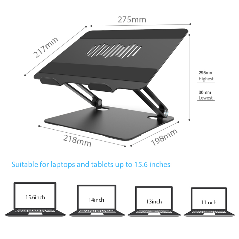
Monitor Stand Riser
Computer Monitor Stand, the multi-point silicone support surface is more non-slip, and the multi-point soft silicone design prevents the computer from scratching while anti-slip. Laptop Stand Amazon is lightweight design, the weight of about 10kgs is equivalent to the weight of a large number of mobile phones, easy to store and go whenever you want.
Shenzhen Chengrong Technology Co.ltd is a high-quality enterprise specializing in metal stamping and CNC production for 12 years. The company mainly aims at the R&D, production and sales of Notebook Laptop Stands and Mobile Phone Stands. From the mold design and processing to machining and product surface oxidation, spraying treatment etc ,integration can fully meet the various processing needs of customers. Have a complete and scientific quality management system, strength and product quality are recognized and trusted by the industry, to meet changing economic and social needs .

Monitor Stand Riser,Metal Desk Monitor Stand Riser,Dual Monitor Riser Stand,Universal Monitor Stand Riser
Shenzhen ChengRong Technology Co.,Ltd. , https://www.laptopstandsupplier.com
