Design engineers working on next-generation communication systems, especially in aerospace, are now pushing the boundaries of what is technologically possible. These systems are becoming more advanced and highly configurable, requiring the integration of multiple functions that were once handled by separate subsystems. This shift offers significant benefits, such as reducing the number of required subsystems, which in turn lowers the overall size, weight, and power consumption (SWaP). However, this approach also introduces new challenges, particularly in supporting cognitive and real-time configuration capabilities.
To address these challenges, the development of high-performance, broadband devices has provided a promising solution. These devices not only meet the performance requirements of various systems but also support a wide range of applications. The ultimate aim for many future systems is to implement a fully software-defined architecture, allowing dynamic changes, field updates, or factory configurations with minimal hardware modifications. This requires the underlying hardware to be flexible enough to support multiple operating modes, each with its own technical specifications.
An example of such a system is a radar and communication platform. These platforms need to handle multi-mode radar operations and electronic support measures (ESM), while also supporting multi-waveform communications and signal intelligence (SIGINT). Integrating both broadband and narrowband functions into a single system can be challenging due to differences in linearity, dynamic range, and other performance criteria. Designers often face trade-offs, such as sacrificing power efficiency or physical size to meet broader frequency coverage needs.
The same issue arises at the device level. For instance, when designing a broadband system, one aspect of the device's performance—such as linearity, noise, or power consumption—may have to be compromised. Table 1 illustrates a typical trade-off between wideband and narrowband phase-locked loops (PLLs) with integrated voltage-controlled oscillators (VCOs). While narrowband devices offer better performance in terms of phase noise and power consumption, they lack the flexibility needed for broader applications.
Table 1. Performance comparison of typical wideband and narrowband PLLs with integrated VCO
Wideband PLL with integrated VCO ADF4351 – Output frequency: 0.035 GHz to 4.4 GHz, Phase Noise: –114 dBc/Hz @ 100 kHz, Power Consumption: 370 mW
Narrowband PLL with integrated VCO HMC837 – Output frequency: 1.025 GHz to 1.150 GHz, Phase Noise: –120 dBc/Hz @ 100 kHz, Power Consumption: 168 mW
Despite the trade-offs involved, the advancement of RF and microwave devices, along with high-speed ADCs, is helping to ease the pressure on system designers. Improvements in CMOS and SiGe processes have enabled more digital functions to be integrated into modern devices. These advancements allow for greater flexibility and advanced signal processing, enabling systems to maintain high performance levels even when reconfiguring for different operating modes.
Figure 1 shows a general-purpose broadband receiver architecture based on recent RF and microwave technologies. Although additional filtering and gain stages may be required in practice, the underlying device’s flexibility supports a wide bandwidth monitoring system. Configurable digital signal processing allows the system to perform narrowband functions when needed and dynamically switch between operating modes, enhancing functionality and adaptability.
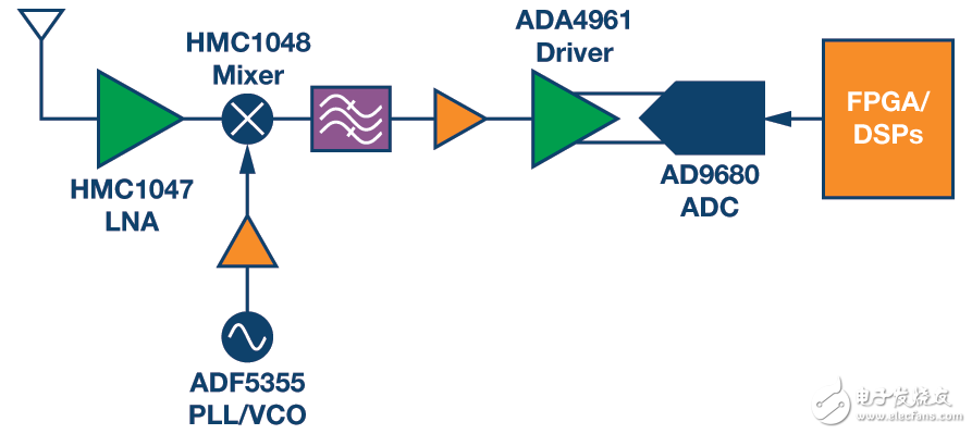
The first two stages of the signal chain use GaAs technology for the low-noise amplifier (LNA) and mixer. While SiGe mixers have improved, front-end devices still benefit from GaAs and GaN components. Devices like the HMC1049 and HMC1048 provide excellent IP3 performance and support both narrowband and wideband operation. These examples show how process advancements enable a single device to meet multiple specifications without relying on extra digital features.
The ADF5355 PLL integrates a VCO that covers a wide frequency range from 54 MHz to 13.6 GHz. It uses four independent VCO cores, each covering 256 overlapping bands, ensuring wide coverage without compromising phase noise or spurious performance. Digital calibration automatically selects the best VCO and band, allowing the system to support both sweeping and fixed frequencies. The device maintains high performance for narrowband applications, with a typical phase noise of –138 dBc/Hz at 1 MHz offset.
The ADA4961 ADC driver delivers wideband performance and excellent linearity. With SPI and embedded digital control, it achieves IMD3 performance of 90 dBc at 500 MHz and –87 dBc at 1.5 GHz. Its digital control options allow for gain adjustment and fast-start settings, optimizing system performance. Fast start improves flexibility by quickly reducing gain when the ADC overloads, preventing saturation.
The AD9680 is a high-speed converter based on a 65 nm CMOS process, supporting up to 1 GSPS at 14-bit resolution. It can undersample IF signals above 1 GHz, aligning with the trend of moving digital conversion closer to the antenna. The device includes digital down conversion (DDC) for customizable output bandwidth, improving SNR and providing flexibility for both wideband and narrowband operations.
The TAD9680 ADC supports both wideband and narrowband functions through its digital signal processing capabilities. When DDC is disabled, it can monitor bandwidths above 500 MHz. When enabled, the NCO digitally mixes the IF signal to baseband and reduces the data rate via a decimation filter. At maximum sampling rates, the output bandwidth can be reduced to 60 MHz, offering greater system flexibility.
While the example focuses on the receiver path, similar devices are available for transmitters. New DACs integrate configurable interpolation filters and digital upconversion functions, making them suitable for broadband RF and microwave applications.
This example highlights how next-generation broadband devices are integrating more digital signal processing and functions, enabling future systems to be dynamically configured for multi-mode operations at unprecedented performance levels. It challenges the belief that narrowband and broadband functions cannot coexist. While some filtering and power considerations remain, the growing availability of high-performance broadband devices and enhanced signal processing makes highly configurable, software-defined systems increasingly viable.
To further illustrate this point, consider the AD9361, an integrated RF IC that demonstrates the blurring of digital and analog functions. It features a direct conversion architecture with built-in digital filtering and calibration, supporting RF input frequencies from 70 MHz to 6 GHz and bandwidths up to 56 MHz. Its configuration capabilities make it ideal for radar, communications, and data link applications.
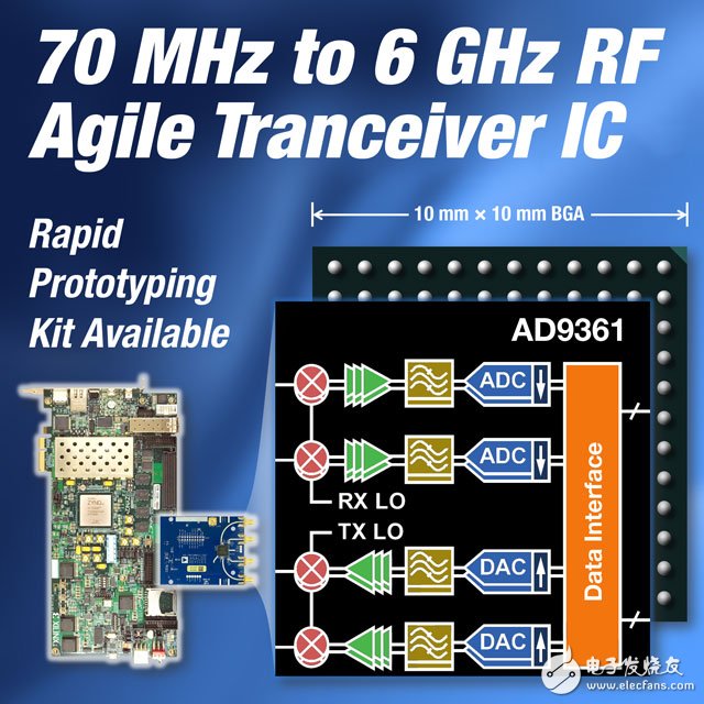
With digital calibration and processing, the AD9361 overcomes many traditional issues of direct conversion systems, offering high integration and configurability. Previously, such levels of integration were unimaginable, and many designers avoided direct conversion due to challenges like image rejection. Today, the increased coupling between digital and analog functions, along with advanced calibration features, enables greater flexibility without significant performance or power trade-offs.
The goal of a fully software-defined system is to have a single RF and microwave signal chain that can support versatile and cognitive applications. While this ideal remains distant, recent developments in semiconductor integration are bringing us closer. Digital signal processing is helping overcome multi-mode challenges, and it may not be long before a single device or cascaded broadband system meets all application needs. The future of software-defined systems looks promising, and we are steadily moving toward that vision.
Fiber Optic Splice Closure,Fiber Optic Splice Case,Fiber Splice Closures,Outdoor Fiber Optic Splice Closure
Cixi Dani Plastic Products Co.,Ltd , https://www.danifiberoptic.com