Specifications such as the US Energy Star require high power factor and high energy efficiency for off-line LED lighting power at any power level. For low-power LED driver power supplies for general lighting, a single-stage power factor correction (PFC) flyback circuit topology based on a dedicated controller IC is the most basic solution. This topology is characterized by the use of only one power switch, eliminating the need for high voltage electrolytic capacitors. For 100~200W LED lighting power supply, people usually use PFC+ flyback two-stage circuit architecture. This topology is characterized by the PFC boost converter being placed at the front end of the flyback converter, and each of the PFC and flyback converters using a power switch. For high-power LED lighting power supplies above 200W, the above two topologies are not applicable. An effective solution is to choose the circuit architecture that combines PFC and its inductor-inductor-capacitor (LLC). In order to achieve high efficiency, the secondary side of the main transformer can adopt a synchronous rectification scheme. Here is an example of a 350W LED lighting power supply design using this solution for your reference.
1 System technical specifications and basic architecture
1.1 350W LED Driver Power Specifications
(1) Input specifications
AC input voltage: 85~264 Vac;
AC maximum input current: 5A;
Line power factor PF: "0.95 (230Vac, full load);
AC power frequency: 47~63Hz;
Efficiency: "92% (230Vac, full load);
Working temperature: 50 ° C;
Working environment: closed;
Cooling method: no fan cooling.
(2) Output specifications
Output voltage Uo: 36~40V;
Output current Io: 5~10A;
Voltage ripple: ≤0.3V;
Current ripple: "0.1A;
Control mode: constant voltage / constant current.
1.2 System composition block diagram
The 350W LED lighting power supply is mainly composed of EMI filter, PFC boost converter based on continuous conduction mode (CCM) power factor controller CM6807, LLC resonant half bridge converter based on CM6900 and synchronous rectifier. Figure 1 is the basic Architecture block diagram.

2 actual circuit
The 350W LED lighting power supply circuit based on CM6807 and CM6900 is shown in Figure 2. We briefly introduce each unit circuit in the system.
2.1 PFC boost converter and auxiliary power supply
The PFC boost converter and auxiliary power supply circuit of the 350W LED lighting power supply are shown in Figure 2(a).
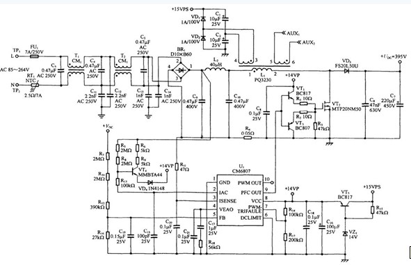
(1) Input stage circuit
The input stage circuit consists of an EMI filter and a bridge rectifier. In Figure 2(a), capacitors C3, C4, C5 and C11~C14 and inductive components T1, T2, etc. constitute the input EMI filter; BR1 is the bridge rectifier; FU1 is the fuse; RT1 is the NTC thermistor. The EMI filter is used to limit and attenuate common mode and differential mode noise. RT1 is used to limit the inrush current caused by charging the large capacitor C7 when the system is started.
(2) Active PFC boost converter
Power factor controller U1 (CM6807), power switch VT2, boost inductor L1, boost diode VD3, input capacitor C9/C10, output capacitor C7, current sense resistor R4, etc., constitute DC/DC active PFC boost Converter. The PFC stage circuit operates in continuous mode. The input current is sensed via U1 pin 2 via R5, R8 and R13. The output DC bus voltage (395V) is sampled by voltage dividers R7, R10, R12, and R13. Pin 4, fed to U1 pin FB.U1, is the voltage error amplifier output, and C17, C18, and C21 are compensation networks. The current through the PFC stage is sensed by R4 and detected by U1 pin 3 via R11 and C20. The drive output on pin 9 of U1 pushes the VT1/VT3 and VT2.PFC boost converters to generate a sinusoidal current that is in phase with the AC input voltage at the input of the bridge rectifier BR1, which meets IEC61000-3. The -2 standard specifies the harmonic current limit requirement, the system power factor is much higher than 0.95, and can output a stable DC voltage of 395V in the AC input voltage range of 85~264V.
(3) Start circuit and bias power supply
R5, R8, R6, R9, VT4, VD4, and C16 form the shoulder circuit on U1 pin 8. Once U1 is started, PFC enters the operating state, and U1 pin 3 is between L1 pins 3 and 4. Auxiliary windings, C1 and C2, VD1 and VD2, R15, VZ1, VT5 and C16 are powered by a bias supply.
2.2 LLC Half Bridge Resonant Power Stage
The LLC half-bridge resonant power stage circuit is shown in Figure 2(b). The power stage main circuit is controlled by the control circuit shown in Fig. 2(c). In Figure 2 (b), the primary inductance between the power switches VT6, VT8, capacitor C23, inductor L3, and transformer T3 pin 3 and pin 6 form a half-bridge LLC series resonant circuit. The VT7 and VT9 on the secondary side of T3 form a synchronous rectifier circuit, which can make the working efficiency of the LLC resonant half-bridge converter more than 96%, which is 4%~5% higher than the efficiency of the traditional LLC resonant half-bridge power stage.

C25/C26, L4 and C27/C28 form an LC filter circuit to ensure that the DC output voltage ripple is less than 300mV. R23 is the output current sense resistor. The DC output of the power supply can drive a 350W LED module or array.
2.3 Constant voltage / constant current (CV / CC) control circuit based on CM6900
The CV/CC control circuit using the CM6900 as a half-bridge resonant controller is shown in Figure 2 (c).
(1) Bias power supply
Figure 2(a) shows the auxiliary winding between L1 pins 5 and 6, and C29/C30, VD7/VD8, VZ2, VT14, R27 and C31 in Figure 2(c), which form a regulated 12V output power supply. Provides bias for U2 (CM6900) and op amp U3 (LM358).
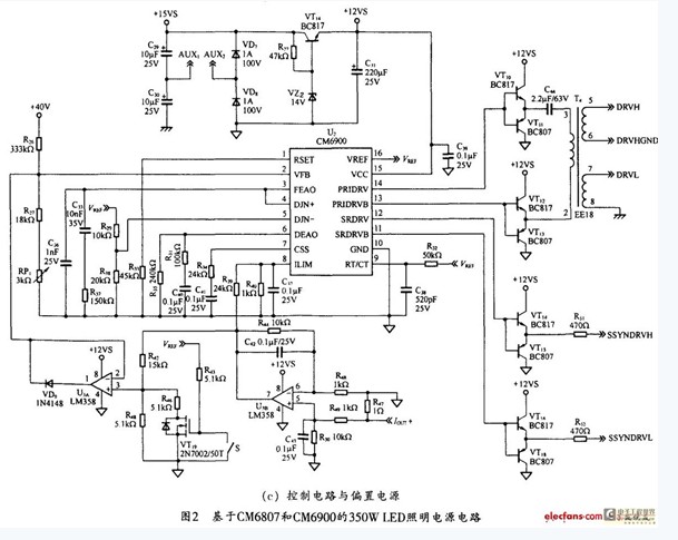
(2) Control and drive circuit
In Figure 2(c), R32 and C38 outside of U2 pin 9 set the oscillator frequency. The output voltage of the LED driver (+40V) is sampled by resistor dividers R26, R27, and PR1 and fed back to pin 2 of U2 to perform output voltage regulation. The current flowing through the output current sensing resistor R23 [see Figure 2(b)] is amplified 150 times by U3B, and after being divided by R42 and R48, U3A is added as a buffer to the feedback loop of the output voltage, so that the output current is Control at a constant value. A switch S is connected between the gate of VT19 and ground. When S is turned off, VT19 is turned on, and the output of U3B is divided by R42 and R48, R46 to 2.5V, so that the LED driving power supply outputs a maximum constant current of 10A. When S is turned on, VT19 is turned off, U3B output is divided by 1.25V to R42 and R48, and the output current of LED driving power supply is 5A.
The outputs on the U2 pins (14) and (13) drive the secondary winding output of the transformer T4.T4 through the transistors VT10/VT11 and VT12/VT13. Figure 2(b) VT6/VT8.U2 in the half bridge The outputs on pins (12) and (13) drive the synchronous rectifiers VT7 and VT9 in Figure 2(b) via VT14/VT15 and VT16/VT18.
3 Conclusion
The CW power factor controller CM6807 and the resonant half-bridge controller CM6900's 350W LED power supply, while using a synchronous rectification scheme, can provide CV/CC control, achieving a power factor higher than 0.95 and an efficiency higher than 90%. The design is suitable for 100~1000W power supply, which can be applied to LED lighting, LED street lights, large LED billboards and stadium LED lighting.
Our Battery Smart Monitoring system is direct integration of the battery restore solution into computer-based battery monitoring system which combines wireless communication with patented, field-proven battery monitor and analysis technology. It not only has the ability to restore battery, but also has the ability to monitor battery's State-Of- Health(SOH) in real time. It is much more intelligent than Smart Pulse Protector and Pulse Restore System because of it's battery remote management and maintenance function with wireless communication.
It is comprised of 3 base hardware which consists of a monitoring host, several monitoring modules, and several data box modules. Plus 1 software operation system. The monitor parts connected wirelessly with batteries pack and reliably reports battery State-Of-Health(SOH) to the software platform.
The battery monitoring system adopts a inspection module for each battery analysis and monitoring. Through the wireless communication technology, every single battery's SOH data collected by monitor is concentrated into the data box module. The data box module is used to collect the battery's voltage, temperature, internal resistance and current simultaneously. Then transmit all the data to the monitoring host which can do data displaying, analysis, storage, and alarming as soon as abnormal. 
Since the Monitoring system is integrated with Base Site Battery Protector System, The real-time improvement of the battery equalization and small pulse current desulfation, lead to the battery lifespan prolonged up to 2 times. Meanwhile, monitor battery's State-Of- Health(SOH) and State-Of-Charge (SOC) in real time to make sure keeping the back up power system always safe and uptime.
Battery Smart Monitoring System
Battery Smart Monitoring System,Battery Monitoring Intelligent System,Battery Intelligent Monitoring System,Battery Remote Monitoring System
Shenzhen Daceen Technology Co., Ltd. , https://www.daceen-sz.com