Author: Samir Cherian
A transimpedance amplifier (TIA) is a front-end amplifier for an optical sensor, such as a photodiode, that converts the sensor's output current into a voltage. The concept of a transimpedance amplifier is simple: the feedback resistor (RF) across the op amp uses Ohm's law VOUT = I &TImes; RF converts the current (I) to a voltage (VOUT). In this series of blog posts, I will show you how to compensate for TIA and how to optimize its noise performance. For a quantitative analysis of key parameters such as TIA bandwidth, stability, and noise, see the application note titled “Transimpedance Considerations for High Speed ​​Amplifiersâ€.
In practical circuits, the parasitic capacitance interacts with the feedback resistor, creating unnecessary poles and zeros in the loop gain response of the amplifier. The most common sources of parasitic input and feedback capacitance include photodiode capacitance (CD), op amp's common mode (CCM) and differential input capacitance (CDIFF), and board capacitance (CPCB). The feedback resistor RF is not ideal and may have a parasitic shunt capacitance of up to 0.2 pF. In high-speed TIA applications, these parasitic capacitances interact with each other and also interact with the RF to generate an undesired response. In this blog post, I will explain how to compensate for TIA.
Figure 1 shows a complete TIA circuit with parasitic input and feedback capacitor sources.
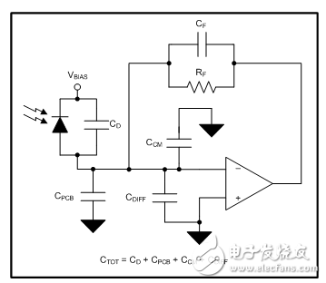
Figure 1: TIA circuit with parasitic capacitance
Three key factors determine the bandwidth of the TIA:
1 Total input capacitance (CTOT).
2 Ideal transimpedance gain set by RF.
3 Operational amplifier gain-bandwidth product (GBP): The higher the gain bandwidth, the higher the resulting closed-loop transimpedance bandwidth.
These three factors are related to each other: for a particular op amp, the positioning gain will set the maximum bandwidth; otherwise, the positioning bandwidth will set the maximum gain.
Parasitic monopole amplifier
The first step in this analysis is to assume that there is a unipolar op amp in the AOL response and the specifications shown in Table 1.
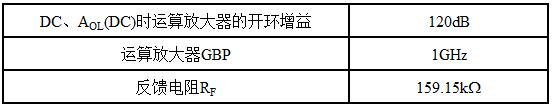
Table 1: TIA Specifications
The closed-loop stability of the amplifier is related to its phase margin ΦM, which is determined by the loop gain response defined as AOL × β, where β is the reciprocal of the noise gain. The TINA-TITM circuit used to determine the operational amplifier AOL and noise gain is shown in Figures 2 and 3, respectively. Figure 2 installs an open-loop configuration of the test equipment (DUT) to derive its AOL. Figure 3 uses an ideal op amp with the required RF, CF, and CTOT to extract the noise gain -1/β. Figure 3 does not currently include parasitic elements CF and CTOT.
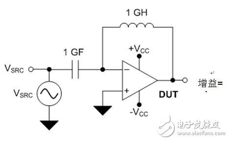
Figure 2: DUT configuration used to determine AOL

Figure 3: amplifier for determining whether the noise over (1 / β) configuration
Figure 4 shows the phase of the analog amplitude and loop gain, AOL and 1/β, respectively. Since 1/β is pure impedance, its response frequency is relatively flat. Since the amplifier is a unity gain configuration as shown in Figure 3, the loop gain is AOL(dB) + β(dB) = AOL(dB). Therefore, as shown in FIG. 4, the AOL and the loop gain curves are in a form of overlapping each other. And because this is a unipolar system, the total phase shift caused by the AOL level under fd conditions is 90°. The final ΦM is 180°-90° = 90° and the TIA is absolutely stable.
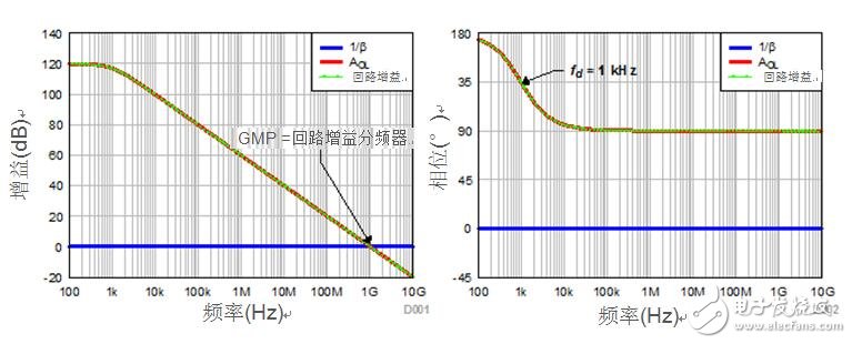
Figure 4: Analog loop gain, ideal for AOL and 1/ β
Influence of input capacitance ( CTOT )
Let's analyze the effect of the amplifier's input capacitance on the loop gain response. Assume that the total effective input capacitance CTOT is 10 pF. The CTOT and RF combination will create a zero on the 1/β curve at a frequency of fz = 1/(2πRFCTOT) = 100kHz. Figures 5 and 6 show the circuit and the resulting frequency response. The AOL and 1/β curves intersect at 10 MHz—the geometric mean of fz (100 kHz) and GBP (1 GHz). The zero point in the 1/β curve becomes the pole in the β curve. The resulting loop gain will have a two-pole response as shown in Figure 6.
The zero point causes the amplitude of 1/β to increase at a rate of 20 dB/decade and intersects the AOL curve at 40 dB/decade proximity (ROC), creating potential instability. The dominant AOL pole exhibits a 90° phase shift in the loop gain at a frequency of 1 kHz. At a frequency of 100 kHz, a phase shift of 90° occurs again at zero frequency fz. The final impact is 1MHz. Since the loop gain crossing occurs only at 10 MHz, the total phase shift of fd and fz will be 180°, resulting in ΦM = 0° and showing that the TIA circuit is unstable.
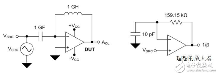
Figure 5: Analog Circuit with 10pF Input Capacitor
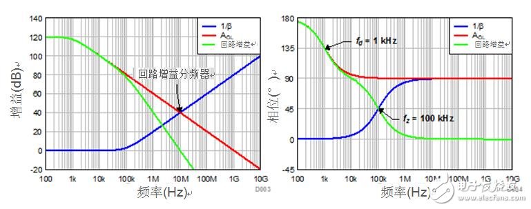
Figure 6: Analog loop gain AOL and (1/β) with input capacitance
Effect of feedback capacitance ( CF )
Add fz to the 1/β response by increasing the capacitance CF in parallel with the RF to recover the phase loss caused by fz. Fp1 is located at 1/(2πRFCF). To obtain the maximum flatness closed-loop Butterworth response (ΦM = 64°), calculate CF using Equation 1: 
Where f-3dB is the closed-loop bandwidth shown in Equation 2: 
Calculated, CF = 0.14pF and f-3dB = 10MHz. Fz is in the ≈7MHz position. The feedback capacitor includes parasitic capacitance from the printed circuit board and RF. To minimize the feedback between the inverting input and output pins of the CPCB removal amplifier, the ground and power planes are traced. Using a small form factor resistor such as 0201 and 0402 reduces the parasitic capacitance generated by the feedback element. Figures 7 and 8 show the circuit and the resulting frequency response.
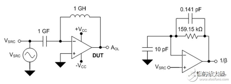
Figure 7: Analog Circuit with 14pF Feedback Capacitor
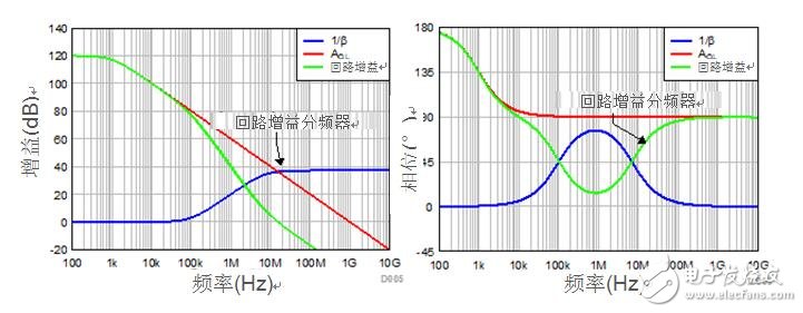
Figure 8: Analog loop gains AOL and 1/β when including input and feedback capacitors
Table 2 summarizes the inflection point in the loop gain response using the Baud curve theory.

Table 2: Effect of pole and zero on loop gain amplitude and phase
1/β curve reached 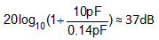 The maximum value. In the Butterworth response, 1/β is at a frequency close to the maximum
 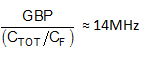 When you meet AOL. Fd and fz form a total phase shift of 180°. The phase regenerated by fp1 is
  This is very close to the simulated 65°.
When designing a TIA, you must understand the capacitance of the photodiode, as this capacitance is usually determined by the application. Once you have determined the capacitance of the photodiode, the next step is to choose the right amplifier for your application.
Choosing the right amplifier requires understanding the amplifier's GBP, the desired transimpedance gain and closed-loop bandwidth, and the relationship between the input and feedback capacitors. You can find an Excel calculator with the equations and theories in this blog post. If you are designing a TIA, be sure to check out this calculator to save you manual calculations and save a lot of time.
Linear Encoder,Digital Linear Encoder,Draw Wire Sensor,1500Mm Linear Encoder
Jilin Lander Intelligent Technology Co., Ltd , https://www.jilinlandertech.com