Voltage is the potential difference
This article refers to the address: http://
Whether you know it or not, anyone who uses an oscilloscope for any voltage measurement is actually making differential voltage measurements. By definition, voltage is an indicator of the potential difference between two points. It is easy for a person using a voltmeter to understand that the voltage is a concept of a potential difference between two points. It is not possible to measure voltage using only one voltmeter lead, but another lead must be connected to provide a reference point. When using an oscilloscope, we sometimes forget that the signal displayed on the oscilloscope is not simply a “signal at that pointâ€, but actually the voltage at that point because it is different from another point.
Reference "grounding" measurement
This other point is usually the grounding of the circuit, which is generally assumed to have a zero voltage. For example, let's assume that we want to use an oscilloscope to measure the voltage on the emitter of the transistor in Figure 1 (reference ground). This may seem like a simple circuit, but from Figure 2 we can see how complex the actual signal measurement environment becomes when we include the oscilloscope probe and the connection between the oscilloscope and the circuit. vA-B represents the transistor emitter voltage waveform we want to display on the oscilloscope. Zcircuit is the resistance of the resistor connected to the emitter in parallel with the emitter impedance of the transistor. We will assign a point as an ideal ground in the circuit to have a solid reference point. ZSCOPE GND is the impedance of the oscilloscope power line ground. ZCOMMON is the impedance between the common point of the circuit and the ideal ground point. iCOMMON indicates that other sources (such as other instruments connected to the circuit under test) flow through ZCOMMON (ground loop) to get vCOMMON.
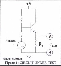
Figure 1: Circuit under test
What the oscilloscope actually displays on the screen is the voltage waveform that is the difference between the input connector center wire voltage and the connector ground voltage or vC-G. In most instances. The displayed waveform vC-G represents to a large extent the signal on the probe stylus vA-B. By examining the various elements of the circuit in Figure 2, we can understand the different ways and reasons why vC-G differs from vA-B.
First, if the values ​​of iCOMMON, ZCOMMON, and ZSCOPE GND are zero, then we don't need to use the probe's ground because there is no voltage difference between the common circuit and the oscilloscope ground. However, these values ​​are not zero, so we have to add a ground connection to the probe to parallel its effects. When the probe ground is connected in parallel with the effects of iCOMMON, ZCOMMON, and ZSCOPE GND, it has its own partial resistance and inductance. We call this impedance ZGND LEAD, which depends on the length of the ground. Part of the current must flow out of the circuit under test and into the oscilloscope input to create a voltage waveform on the oscilloscope that performs the measurement. The signal current ZGND LEAD flowing through the ground impedance of the probe causes the voltage to drop, making vC-G different from vA-B. To illustrate this effect, Figure 3 shows a square wave measured using an oscilloscope and a compensated standard oscilloscope probe. The first waveform is measured using the probe stylus adapter, which minimizes the length of the ground connection. The second and third waveforms were measured using the same device, but 36cm (14") and 58cm (23") ground wires were used on the probe. In many measurements, signal damage caused by ground impedance may be acceptable, but it is important to know that such signal damage is present. Looking again at Figure 2, when iCOMMON flows through ZCOMMON, it forms what we call vCOMMON. If the oscilloscope probe is not connected, vCOMMON will be represented as the "common" voltage for points A and B. The voltage waveform at any point relative to the ideal ground will include vCOMMON. Point B is equal to vCOMMON, and point A is equal to vA-B + vCOMMON. By using the oscilloscope probe ground to point B, we can reduce, but not eliminate, vCOMMON from the measurement. The reason we can't eliminate vCOMMON is that the value of ZGNDLEAD is finite.
ZGNDLEAD, ZCOMMON, and ZSCOPEGND form a loop through which iCOMMON will flow. The voltage caused by iCOMMON flowing through this loop will further destroy the waveform vC-G.

Figure 2: Measured circuit connected using an oscilloscope
"Ungrounded" reference measurement
By turning on the safety ground on the oscilloscope, you can usually reduce the impact of iCOMMON. Depending on the magnitude of vCOMMON, this technique can be very dangerous and is not recommended under any circumstances. Turning on the oscilloscope's safe ground does not eliminate iCOMMON flowing through the ZGND LEAD because ZSCOPE GND is in parallel with the oscilloscope transformer's complex impedance, while the oscilloscope's transformer's mutual capacitance is in series with the power system's impedance, Z POWER TO GND. The vCOMMON model we use also explains the measurement limits that we typically consider when making "floating" measurements. We assume that vCOMMON is the output of the iCOMMON low-impedance voltage supply to be passed through, such as when trying to measure the voltage in the "floating" power control circuit where vCOMMON is the power line voltage. Even if it is safe to open a safe ground floating oscilloscope, vCOMMON is the capacitance and power line impedance effect of the iCOMMON of the power line voltage flowing through the oscilloscope transformer, which will still damage the measurement results. In addition, as in the previous reference grounding measurement example, the signal current flowing through ZGNDLEAD will also damage the signal. In addition, there is a less relevant issue: floating the oscilloscope chassis to the line-level voltage may generate more voltage between the primary and secondary coils of the oscilloscope transformer that is designed to handle the oscilloscope.
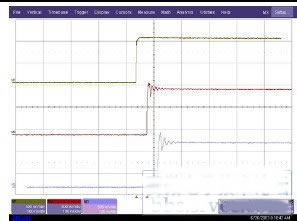
Figure 3: Impact of the probe ground
Differential voltage measurement
These damaging measurement effects can be greatly reduced by using an oscilloscope or preamplifier with differential measurement. Figure 4 shows the equivalent circuit and the same reference grounded oscilloscope and differential amplifier. The ideal differential amplifier only amplifies the difference seen on the + input and - input. This is very similar to a voltmeter, we will probe two points and find the voltage difference between the two points. When the differential amplifier amplifies the difference between two points, it suppresses any voltage shared by the two points. Since vCOMMON appears at both points A and B of our circuit, the differential amplifier suppresses this voltage, indicating the difference between point A and point B, vA-B, for the oscilloscope.
(v AB + vCOMMON) - (vCOMMON) = v AB
Since the high impedance of the probe prevents vCOMMON from generating the sensed current in the oscilloscope ground, it also greatly reduces the loop current impact of vCOMMON. Since the probe ground clip is not connected to point B, the effect of ZGND LEAD is eliminated. Therefore, vC-G represents VA-B to a much greater extent than using the oscilloscope probe ground to provide a negative reference. Because a differential amplifier with a properly designed probe can reject a relatively high amplitude common voltage, high-quality measurements can be made without floating the oscilloscope to an unsafe level.
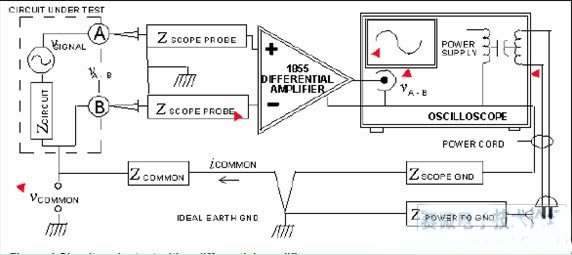
Figure 4: Measured circuit using a differential amplifier
Common mode rejection ratio or CMRR
We have already discussed the benefits of using an ideal differential amplifier for voltage waveform measurements. Unfortunately, the ideal differential amplifier does not exist, we must understand some of its features and limitations. Looking at Figure 4 again, we can see that the differential amplifier processes two voltage waveforms: one we want to see and one that we don't want to see. We can call them the differential mode waveform (the difference between point A and point B) and the common mode waveform (shared between point A and point B). The waveform we want to see is the differential mode signal vA-B. All features of a single-ended amplifier, such as gain and bandwidth, apply to the differential mode signal of a differential amplifier. If you need an oscilloscope with 50MHz bandwidth and enough gain to adequately measure the reference ground signal, such as vA-B, then you need a differential amplifier that has the same functionality in differential mode. As mentioned earlier, a common-mode signal, vCOMMON, can be processed using a single-ended oscilloscope by applying a low-impedance shunt (ZGNDLEAD) or by placing an impedance in series with the common-mode signal (floating oscilloscope). The differential amplifier processes the common mode signal by subtracting the common mode signal from the measured differential signal. Similarly, differential bandwidth and gain can be used to indicate the ability of a differential amplifier to cancel or reject a common-mode signal, but what we want now is attenuation, not gain. The common mode bandwidth can be measured by applying the exact same signal (frequency, amplitude, and phase) to both inputs of the differential amplifier. For these input signals, the ideal differential amplifier does not have any signal on the output. Since the actual environmental limitations also apply to the actual amplifier, there will be an output that is related to the amplitude and frequency of the input signal. If we put a 1 V, 10 MHz signal into two inputs simultaneously, the differential amplifier may reject the 1 MHz signal with a factor of 1,000. The ability of a differential amplifier to reject a common-mode signal is typically expressed as the ratio of the amplitude of the input signal divided by the amplitude of the differential input signal or the common-mode rejection ratio (CMRR). In this example, the CMRR at 10 MHz is 1,000:1. It is usually expressed in terms of attenuation (dB), but it is always the ratio of the output amplitude to the input amplitude. This indicator should be specified relative to the attenuation ratio as a function of frequency as it varies with frequency. CMRR is highest on DC and decreases as frequency increases.
Common mode range
The second important feature of the differential amplifier we need to know is the common mode range, which indicates the maximum vCOMMON amplitude that the amplifier can tolerate. This value is usually at least several times larger than the differential input range and is specified as a DC value, but it also applies to the peak amplitude of the AC signal. How large the common mode range the differential amplifier should be depends on the measurement requirements. If the common mode voltage is a small signal caused by the ground loop current, then a range of one or two volts is sufficient. However, if the differential signal to be measured is at the top of a large common mode voltage, then this range must be large. For example, let's assume that vA-B is the voltage waveform in the current-sense resistor of the switching power supply primary circuit. In this example, vCOMMON is 400 V (DC + peak AC), and the v AB waveform is a voltage ramp with a peak of 1 V. . By using a probe and attenuator with a 10 integrated attenuation coefficient, vCOMMON will attenuate to 4 V and vA-B will attenuate to a 10 mV signal. The differential amplifier must have a common mode range of at least 4 V.
If the amplifier's CMRR is 10,000:1, the differential amplifier will attenuate 4 V vCOMMON to 400 μV on the output. In this case, the CMRR of the amplifier is combined with the attenuation of the probe and the internal attenuator of the amplifier. The common mode signal is attenuated by 1,000,000:1 and the differential signal is attenuated by a factor of 100. This output can be easily and safely displayed on a standard ground reference oscilloscope.
Get good CMRR
Good common-mode rejection ratio performance can be achieved by carefully matching all of the properties of the + and - signal paths flowing into and through the differential amplifier. This matching is very important for both the probe and the amplifier.
Some oscilloscopes obtain CMRR (commonly referred to as AB) by subtracting one input from the other. In an analog oscilloscope, this is done by reversing one channel and then adding it to another channel in the oscilloscope input section. Digital oscilloscopes (DSOs) provide a variety of digital functions that can subtract one waveform from another.
DSOs typically do not specify CMMR for such operations, but DC coefficients can be derived by considering the accuracy metrics for each channel. If the DC gain accuracy of each channel is ±1%, then the CMRR may be as low as 50:1, rarely better than 100:1. The CMRR will deteriorate further when considering the AC signal. In our first 1 V signal example on top of the 400 V common-mode signal, a 10mV differential signal and a 40mV common-mode signal are output. In addition, the input cannot tolerate a bias level of 4 V.
To achieve optimal CMRR, the probe used in the differential amplifier should be designed to maximize CMRR. The user needs to ensure that the probe is compensated in an optimal way.
The FirstPower gel battery uses the sealed gel technology and is designed for high reliable, maintenance-free power for renewable energy applications. Depending on the advantage gel technology, optimum grid and plate design, the FirstPower gel battery offers highest power and reliability for your equipments.Gelled electrolyte, no flow, no leakage or no gradation of sulfuric acid.
The positive plate is tubular plate, which can effectively prevent the active materials from falling off.PVC-SiO2 separator, which is special for gel battery with tiny holes.
The separator has high volume porosity, low electrical resistance and excellent wettability
Maintenance-free during the whole service life.
Low self discharge rate
Proof against deep discharge according to DIN 43539 T5
Main Power Opzv Battery,Dischargeable Main Power Opzv Battery,Opzv Battery For Mains Power
Firstpower Tech. Co., Ltd. , https://www.firstpowersales.com