Abstract: This paper introduces the control unit of highway vehicle detection system designed by ARM7 core microprocessor LPC2114. It focuses on the design of large-capacity flash memory unit and the related matters of ARM development. The system principle block diagram, unit circuit design and Software design ideas.
This article refers to the address: http://
introduction
Due to the increasing traffic demand, more and more ring induction coil detectors are used for traffic detection. These coils buried under the surface of the road can detect the electromagnetic changes when the vehicle passes and accurately calculate the traffic flow. Traffic flow is the basic data of traffic statistics and traffic planning. These test results can be used to calculate the occupancy rate (characterizing traffic density). When using the dual coil mode, it can also provide data such as speed, vehicle driving direction, and vehicle classification. Data is extremely important for traffic management and statistics. Generally, the highway vehicle detection system consists of a multi-channel ring detection unit LD4 and a control unit CCU. This paper uses the latest ARM7 core microprocessor LPC2114 from PHILIPS to design the control unit of the vehicle detection system, and five LD4 ring detectors. Together form a 10-channel highway vehicle detection system.
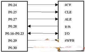
LPC2114 and electronic hard disk connection diagram
Main program flow chart
Overall design
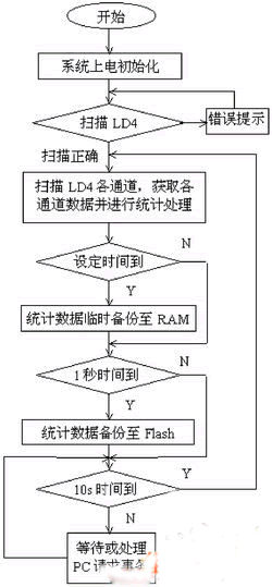
The schematic diagram of the control panel system designed in this paper is shown in Figure 2. The LPC2114 is the core control unit. The chip is a 16/32-bit ARM7TDMI-S core-based CPU that supports real-time simulation and tracking. It integrates four 10-bit A/D converters, two 32-bit timers, a real-time clock and watchdog, multiple serial interfaces, including two industry-standard UARTs, high-speed and two SPI bus interfaces. Up to 46 external TTL-compatible general purpose I/O ports are ideal for use as a master unit. The CPLD EPM7128 acts as an extended input/output for the microprocessor and is connected via optocoupler to the LD4 standard definition bus. The standard defined bus is based on the RS-485 bus communication protocol. The LD4 and the control board exchange data through the standard bus. The control board scans and sends a command requesting data every 10 seconds. The corresponding LD4 channel returns request data or invalid information, and the ARM processor performs corresponding statistical operations on each channel data obtained. deal with. The statistical data is stored in the static RAM every time set by the user for the central station to acquire regularly, and the statistical data is backed up to the Flash electronic hard disk in minutes. The central station can obtain the data of the corresponding time period by requesting the backup data command and store it in the database. The central station and the control board communicate by RS-232 serial port, and remote data transmission is realized by using a modem. In order to solve the problem of large-capacity storage, the system uses the K9F2808 provided by Samsung as an electronic hard disk, 16MB of capacity can store 11 days of backup data, and the electronic hard disk can be flexibly upgraded.
Interface between LPC2114 and electronic hard disk
In order to prevent data loss caused by transmission and central station failures, the system requires backing up data for a period of time. Therefore, large-capacity storage problems need to be considered in the process of system design.
Set the system to back up the statistics every minute. According to the data format of the ring detector LD4, the data amount is 1026B. If static RAM is used as the storage unit, multiple large-capacity RAM cascades are needed, which is expensive and storage. Capacity expansion is difficult. If dynamic RAM is used as the storage unit, the disadvantage is that the control is difficult and the dynamic RAM controller is required to assist the operation. Flash is simple to use as a memory and has a large capacity. Although the service life is limited, considering that the system stores 1026B every 1 minute, in terms of 16MB capacity, it is written once every 11 days, then it is erased about 3 times a month. The era is erased about 36 times, and the life of Flash is generally more than 100,000 times, so the system can use Flash as an electronic hard disk in the vehicle detection system. In addition, Flash also has a power-down non-volatile feature, which is more suitable for the system.
In order to facilitate the upgrade and expansion of storage capacity, the system uses K9F2808 as the memory. K9F2808 is a 48-pin surface-mount device. The chip has (16M+512K)×8 bit memory space inside, which can form 32768 rows and 528 columns. The reserved 16-column column address code is 513~527, which can be 528 bytes. Read and write for one page and 32 pages for one erase operation. In addition, the K9F2808 is characterized by its command, address and data information transmitted through eight I/O buses. The interface standard is uniform and easy to upgrade storage capacity.
The connection between the LPC2114 and the Flash electronic hard disk is as shown in the figure. Since the LPC2114 does not have an external bus, only the I/O operation mode can be used for the Flash operation. The K9F2808 has the common features of various operations, that is, the operation command word is first sent to the command register on the I/O port, and the address of the operation unit is sent for three consecutive cycles, in the order: A0~A7, A9~A16, A17~ A23, where A8 is determined by the command word.
Take the page programming operation as an example to give the K9F2808 ARM driver (based on the ADS1.2 development environment), and the page read and block erase methods are similar to page programming, except that the read is by the #RE signal to latch the data. Only two cycles of address must be sent when erasing.
Row_add is the page number, which needs to be shifted 9 bits to get the row address. Erase_flash( ) - Erase Flash function
Write_command( ) - write command function
Write_address( ) - write address function
Write_data( ) - write data function
Read_data( ) - read data function
Void flash_store(uint32 row_add, uint8 *buffer )
{ uint16 i;
Uint32 statue,address;
//Variable definitions
IO0DIR |= 0x00ff0000;
/ / Set the IO direction
If((row_add== 0)|| ((row_add%32)==0))
{address = row_add<<9;
Address &= 0x00fffe00;
Erase_flash(address);}
/ / Erase Flash
Write_command(0x80);
/ / Write command 80H
Address = row_add<<9;
Address &= 0x00fffe00;
Write_address(address);
/ / write address
Statue = IO0PIN;
/ / Get the status
While((statue&fr_b)==0)
{statue = IO0PIN;}
//Busy, wait
For(i=0;i<528;i++)
/ / Write 528 bytes
{write_data(*(buffer+i));}
//data input
Write_command(0x10);
/ / Write command 10H
Statue = IO0PIN;
/ / Get the status
While((statue&fr_b)==0)
{statue = IO0PIN;}
//Busy, wait
Write_command(0x70);
/ / Write command 70H
Statue = read_data();
/ / Get the status
If(statue&0x01)
{IO0SET |= errorled;}
//operation failed
}
LPC2114 serial communication implementation
The control system uses the two UARTs of the LPC2114 to implement data exchange with the LD4 and the central station. The two UARTs have a 16B transceiver FIFO with adjustable trigger points. Among them, UART1 adds a modem interface to UART0. The basic operation of the UART is similar to the traditional 51-core microcontroller.
First, set the I/O connection to the UART; then set the serial port baud rate (such as U0DLM, U0DLL); then set the serial port working mode (such as U0LCR, U0FCR); then you can send/receive data through the registers U0THR and U0RBR. The status information of the transmit/receive module can be read via the U0LSR register.
The system communicates with the LD4 board through the RS-485 bus, and uses the MAX3485 as the RS-485 bus controller and the UART1 communication of the LPC2114. The MAX3485 is a 3.3V-powered half-duplex transceiver chip that converts differential RS-485 bus signals into serial signals that the ARM core can accept. In order to communicate with the PC, the system uses the MAX3232 with 3.3V operating voltage as the RS-232 level conversion chip.
LPC2114 design considerations
LPC2114 has some special issues in the development process, summarized as follows:
(1) When the user program cannot be run after writing to Flash, first, it is necessary to consider whether the interrupt vector table is correct, and the interrupt vector table accumulation sum must be 0. Second, you need to consider the positioning of the vector table, whether the vector table has been located at 0x00000000 address. Then, you need to consider whether the MEMMAP register settings are correct, otherwise the interrupt cannot be executed. In addition, it is also necessary to consider whether the ISP hardware condition is satisfied. When the P0.14 pin of the LPC2114 is low at #RESET, the low level on the pin line will force the chip to enter the ISP state, and the hardware design must add 10KW to the pin. Pull-up resistor, otherwise, this pin is unstable and will have an effect on device startup.
(2) The LPC2114 has a total of 46 GPIOs. These I/Os can be arbitrarily configured, but the individual pins have open-drain outputs (P0.2, P0.3), plus pull-up resistors. In addition, the flash memory K9F2808 status output pin R / #B open drain output, need to add 10KW pull-up resistor.
(3) After the LPC2114 chip is encrypted, the JTAG debugging and downloading functions can be restored only after the chip is globally erased by the ISP. When #RESET is low, the low level of P1.26 makes P1.26~P1.31 reset as the debug port. Note that a weak bias resistor should be connected between P1.26 pin and ground.
System software design ideas and precautions
The vehicle detection system ARM software adopts the layered design idea, and the whole software consists of two parts: driver and application software. The driver part encapsulates Flash operations, RS-485 operations, real-time clock (RTC) operations, RS-232 operations, and I/O. The application software is divided into a basic function library and a main program.
In the 32-bit ARM core application system, in order to perform system initialization, an assembly file is often used as the startup code to implement stack, interrupt, system variables, I/O initialization, and address remapping. The strategy for developing platform ADS is to not provide complete startup code, and the lack of it needs to be written by developers themselves.
The startup code of the system design includes the interrupt vector table, stack initialization, and the interface between the corresponding interrupt service program and C language. For LPC2114, in order to make the 32-bit accumulation sum of all data in the vector table to 0, the reserved vector value is set in the vector table, and the 32 bytes in the interrupt vector table are accumulated, wherein the reserved vector values ​​are not accumulated, and then The complement of the accumulated value, the lower 32 bits of this complement is the value of the reserved vector. This reserved vector value will be used as a valid user program key by the BOOT loader. When all the accumulated sums of data in the vector table are 0, and the external hardware conditions of the ISP are not satisfied, the BOOT loader will execute the user program.
Conclusion
This paper is based on PHILIPS' latest ARM7 core microprocessor LPC2114 to realize the design of the control unit part of the highway vehicle detection system. The LPC2114 is easy to use, easy to develop, and cost-effective, making it ideal for embedded systems. At present, the system has been introduced to the market and has achieved good economic benefits.
Storm Circuit has been producing Multilayer PCBs for over 10years. Over the years, we have seen all types of multilayer constructions from various industries, answered all types of multilayer questions, and solved all types of problems with multilayer PCBs.
Multilayer PCB is a circuit board with two or more layers. The material unlike Double-Sided PCBs with only two conductive layers all multilayer PCBs is that it must have at least three layers of conductive material, and the PCB boards are buried in the center of the material.
Benefits of Multilayer PCBs (compared to single or double-sided PCBs)
Higher assembly density
Smaller size (considerable savings on space)
Increased flexibility
Easier incorporation controlled impedance features.
EMI shielding through careful placement of power and ground layers.
Reduces the need for interconnection wiring harnesses (reduces overall weight
Multilayer PCB
Multilayer PCB,Multilayer Bga Board,Multilayer Smd PCB,Multilayer Circuit Board PCB
Storm Circuit Technology Ltd , http://www.stormpcb.com