The production process of epitaxial wafers is very complicated, and the detection process is also relatively complicated. The basic method is to randomly select nine points for each epitaxial wafer for testing. Those that meet the requirements are good products, others are bad products (large voltage deviation, short wavelength Or longer, etc.). Good quality epitaxial wafers will start to be electrodes (P pole, N pole), then cut the epitaxial wafer with laser, and then pick it up 100%, according to different voltages, wavelengths, brightness, fully automated sorting, which is formed LED chip (square piece). Then, visual inspection is needed to sort out any defects or worn electrodes. These are the scattered crystals behind. At this time, there is a wafer on the blue film that does not meet the normal shipping requirements, and it naturally becomes an edge piece or a wool piece. Defective epitaxial wafers (mainly because some parameters do not meet the requirements), they are not used for square wafers, they are directly used for electrodes (P-pole, N-pole), and no sorting is done, which is the current LED circle Film (there are also good things in it, such as square films, etc.).
Semiconductor manufacturers mainly use polished Si wafers (PW) and epitaxial Si wafers as raw materials for ICs. In the early 1980s, epitaxial wafers were used, which had certain electrical characteristics not found in standard PWs and eliminated many surface / near-surface defects introduced in crystal growth and subsequent wafer processing.
Historically, epitaxial wafers have been produced and used by Si wafer manufacturers for their own use. They are not used in large amounts in ICs. It requires the deposition of a thin single crystal Si layer on the surface of single crystal Si wafers. Generally, the thickness of the epitaxial layer is 2 to 20 μm, and the thickness of the substrate Si is 610 μm (150 mm diameter plate and 725 μm (200 mm plate).
The epitaxial deposition can process multiple pieces at the same time (simultaneously) or single pieces. The monolithic reactor can produce the best quality epitaxial layer (thickness, resistivity uniformity, and few defects); this epitaxial wafer is used for the production of 150mm "frontier" products and all important 200mm products.
Extension products
The epitaxial products are used in four aspects, and CMOS complementary metal oxide semiconductors support cutting-edge processes that require small device sizes. CMOS products are the largest application area of ​​epitaxial wafers, and are used by IC manufacturers for non-recoverable device processes, including microprocessors and logic chips, and flash memory and DRAM (dynamic random access memory) for memory applications. Discrete semiconductors are used to manufacture components that require precise Si characteristics. The "exotic" semiconductors include special products that use non-Si materials, many of which are compound semiconductor materials incorporated into the epitaxial layer. The buried layer semiconductor is physically isolated using heavily doped regions in the bipolar transistor element, which is also deposited in the epitaxy process.
Currently, in 200mm wafers, epitaxial wafers accounted for 1 / 3.2000, including the buried layer, CMOS for logic devices accounted for 69% of all epitaxial wafers, DRAM accounted for 11%, discrete devices accounted for 20%. By 2005, CMOS Logic will account for 55%, DRAM for 30%, and discrete devices for 15%.
LED epitaxial wafer: substrate material
Substrate materials are the cornerstone of technological development in the semiconductor lighting industry. Different substrate materials require different epitaxial growth technology, chip processing technology and device packaging technology. The substrate material determines the development route of semiconductor lighting technology. The choice of substrate material mainly depends on the following nine aspects:
1. Good structural characteristics, the crystal structure of the epitaxial material and the substrate is the same or similar, the lattice constant mismatch is small, the crystallization performance is good, and the defect density is small;
2. The interface characteristics are good, which is conducive to nucleation and strong adhesion of epitaxial materials;
3. Good chemical stability, not easy to decompose and corrode in the temperature and atmosphere of epitaxial growth;
4. Good thermal performance, including good thermal conductivity and low thermal mismatch;
5. Good conductivity, can be made up and down structure;
6. The optical performance is good, and the light emitted by the manufactured device is absorbed by the substrate less;
7. Good mechanical properties and easy processing of the device, including thinning, polishing and cutting;
8. Low price;
9. Large size, generally require a diameter of not less than 2 inches.
It is very difficult to choose the substrate to satisfy the above nine aspects at the same time. Therefore, at present, it is only possible to adapt to the development and production of semiconductor light-emitting devices on different substrates by changing the epitaxial growth technology and adjusting the device processing technology. There are many substrate materials for GaN research, but there are currently only three substrates that can be used for production, namely sapphire Al2O3 and silicon carbide SiC substrates and Si substrates.
Smd335 Led Strip Light Introduction:
1.SMD335 Led Strip light bar
2. Size: Length Width 8mm 1000*
3.LED specification: 335SMD*60PCS
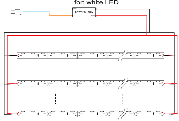
4. Voltage: DC12V
5. Power: 3.6W
6. Luminous flux: 270-300LM
7. Color: White (various colors red, yellow, green, blue, amber, etc. can be)
8. Packing: card loaded or static bag
9. Warranty: One year (under normal use)
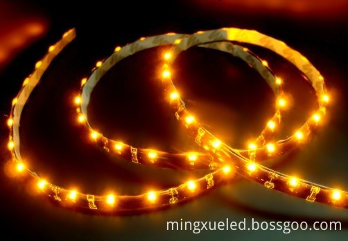
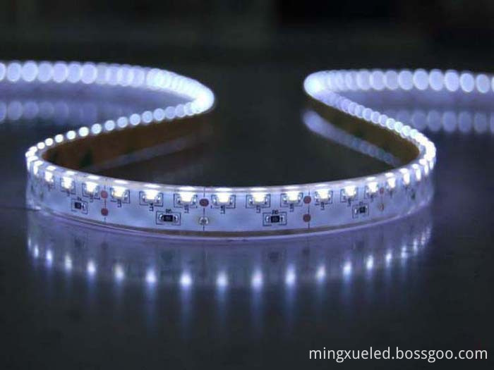
SMD335 Led Strip Light Product Features:
1. The use of very soft PCB board as a substrate, ultra-bright SMD LED as luminous body.
2. SMD335 LED Strip Light can be bent, stable and reliable quality
3. Every three LED as a group, can be based on the length requirement, cut in between each unit
4. The anti-oxidation, anti-ultraviolet radiation and long-term use does not change color
5. The silicone transparent waterproof connector can easily connect and totally waterproof
6. IP water level (optional IP68, IP66, IP65,) optional
use:
SMD335 Led Strip Light can be used in interior decoration, automotive lighting and other projects.
We focus on LED area, is a high-tech lighting enterprise deal in develop, produce and sales.

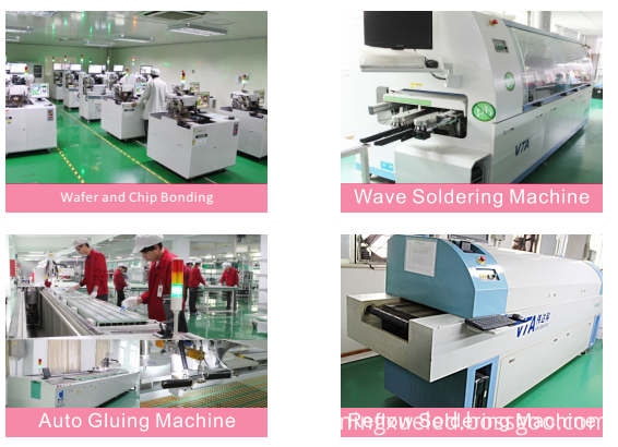
Owns DIP LED, SMD LED professional production lines and LED lighting products lines, the produce volume per month for DIP LED,SMD LED is 50 million pieces, for LED flexible strip light is 500 thousands meters, for SMD335 Led Strip Light for car is about 200 thousands pairs, for LED tube light is 50 thousands pieces, for LED Spotlights are 200 thousands pieces, for LED ceiling light are 50 thousands pieces.
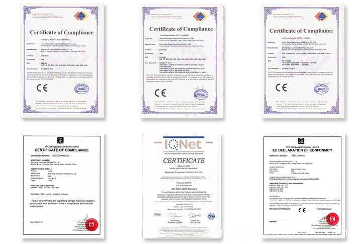
Mingxue Optoelectronics Co.,Ltd. has apply the I S O 9 0 0 1: 2 0 0 8 international quality management system certificate, for SMD335 Led Strip Light, we apply the CE, RoHS and SAA certificate for our led lighting product.
Our R & D team can handle highly customized designs and offer OEM and ODM services.
We hope to set up a long-term partnership with you through our high quality products and our Sincere Service!
SMD335 Led Strip Light
Smd335 Led Strip Light,12V Smd335 Led Strip Light,Smd335 Led Strip Light Waterproof,High Lumen Smd335 Led Strip Light
Shenzhen Mingxue Optoelectronics CO.,Ltd , https://www.led-lamp-china.com