Based on recent trends, increasing efficiency has become a key goal, and the trade-offs of using slow switching devices to achieve better EMI are not worthwhile. Super junctions increase efficiency in applications where planar MOSFETs are difficult. Super-junction MOSFETs significantly reduce on-resistance and parasitic capacitance compared to traditional planar MOSFET technology. The significant reduction in on-resistance and the reduction in parasitic capacitance, while contributing to efficiency, also result in fast switching of voltage (dv/dt) and current (di/dt), resulting in high frequency noise and radiated EMI.
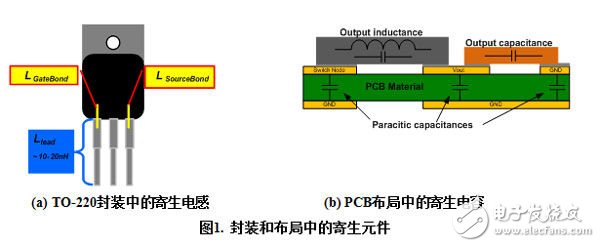
To drive fast-switching super-junction MOSFETs, it is important to understand the effects of package and PCB layout parasitics on switching performance and PCB layout adjustments for using super-junctions. A super-junction MOSFET with a breakdown voltage of 500-600V is mainly used. Among these voltage ratings, the industry standards TO-220, TO-247, TO-3P and TO-263 are the most widely used packages. The impact of the package on performance is limited because the internal gate and source bond line lengths are fixed. Only the length of the pin can be changed to reduce the source inductance of the package. As shown in Figure 1(a), the typical lead inductance of 10nH does not seem to be large, but the di/dt of these MOSFETs can easily reach 500A/μs! Assuming di/dt is 500A/μs, the voltage on the 10nH lead inductor is VIND=5V; and the turn-off di/dt of the 10nH lead inductor is 1,000A/μs, which produces a voltage of VIND=10V. Most applications and designs do not take into account that this additional inductor will also generate voltage, but this can not be ignored. The above simple calculations show that the total source inductance of the package, ie the bond line and pin inductance, must be reduced to an acceptable value. Another source of noise is layout parasitics. There are two visible layout parasitics: parasitic inductance and parasitic capacitance. The inductance of the 1cm trace is 6-10nH, which can be reduced by adding a layer on top of the PCB and adding a GND layer on the bottom of the PCB. The other type is parasitic capacitance. Figure 1(b) shows the principle of capacitive parasitic effects in the layout. The parasitic capacitance is caused by the distance between two adjacent traces or between the trace and the ground plane on the other side. Another type of capacitor is the capacitance between the device and the ground plane. Two parallel lines on both sides of the PCB increase capacitance and reduce loop inductance, thereby reducing electromagnetic noise emissions. Consider these layout tips when the next design requires a super-junction MOSFET.

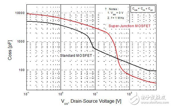
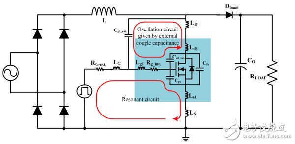
Because MOSFETs are unipolar devices, parasitic capacitance is the only limiting factor for switching transients. The charge-balancing principle reduces the on-resistance of a particular area and, compared to standard MOSFET technology, the chip size is the same under the same RDS(ON). Figure 1 shows the capacitance of a super-junction MOSFET and a standard planar MOSFET. The Coss of a standard MOSFET has a moderate linear relationship, while the Coss curve of a super-junction MOSFET exhibits a highly nonlinear relationship. Because of the higher cell density, the Coss initial value of the super-junction MOSFET is higher, but in the super-junction MOSFET, Coss will drop rapidly near the drain-source voltage of about 50V, as shown in Figure 2. These nonlinear effects can cause voltage and current oscillations when using super-junction MOSFETs applied to PFC or DC/DC converters. Figure 3 shows a simplified schematic diagram of a PFC circuit, including a parasitic element inside the power MOSFET and an external oscillating circuit that includes an external coupling capacitor Cgd_ext.

Figure 2. Comparison of planar MOSFET and super-junction MOSFET output capacitors
In general, multiple oscillator circuits affect the switching characteristics of the MOSFET, including internal and external oscillator circuits. In the PFC circuit of Figure 3, L, Co, and Dboost are inductors, output capacitors, and boost diodes, respectively. Cgs, Cgd_int, and Cds are the parasitic capacitances of the power MOSFET. Ld1, Ls1, and Lg1 are the drain, source, and gate bonding lines of the power MOSFET and the pin inductance. Rg_int and Rg_ext are the internal gate resistance of the power MOSFET and the external gate drive resistance of the circuit. Cgd_ext is the parasitic gate-drain capacitance of the circuit. LD, LS, and LG are the stray inductance of the drain, source, and gate traces of a printed circuit board (PCB). When the MOSFET is turned on or off, the gate parasitic oscillation occurs in the resonant circuit through the gate-drain capacitance Cgd and the gate lead inductance Lg1.

Figure 3. Schematic of a PFC circuit with external parasitic components inside the power MOSFET
Under the resonant condition (ωL = 1 / ω C), the oscillating voltage generated in the gate and source voltages is much larger than the driving voltage. The voltage oscillation due to the resonance change is proportional to the quality factor, Q (= ωL / R = 1 / ωCR). When the MOSFET is turned off, the drain parasitic inductance (LD+Ld1), the gate-drain capacitance Cgd, and the gate lead inductance Lg1 network cause the gate oscillating voltage. If the gate resistance (RG-ext.+Rg_int.) is extremely small, Q becomes large. In addition, the voltage drop across the LS and the Ls1 source stray inductance oscillate in the gate-source voltage, which can be expressed by the expression (1). Parasitic oscillations can cause gate-source breakdown, poor EMI, large switching losses, gate control failure, and even MOSFET failure.

It is important to optimize the circuit design to maximize the performance of the super-junction MOSFET without negative effects.
The FirstPower gel battery uses the sealed gel technology and is designed for high reliable, maintenance-free power for renewable energy applications. Depending on the advantage gel technology, optimum grid and plate design, the FirstPower gel battery offers highest power and reliability for your equipments.
Reserve Gel Battery,High Efficiency Reserve Gel Battery,Pvc Gel Battery,Gel Cell Battery
Firstpower Tech. Co., Ltd. , https://www.firstpowersales.com