FPGA's rich logic resources, abundant I/O pins, and low power consumption are widely used in embedded systems and high-speed data communications. Nowadays, major FPGA manufacturers provide more and available IP core resources for user-friendly design and use, which greatly reduces the product development cycle and development difficulty, so that users can conceive more A variety of creative and practical features, rather than wasting a lot of time on product debugging and verification.
The application of Gigabit Ethernet technology in engineering is one of the current research hotspots. Compared with other serial communication such as RS-232 or RS-485, Gigabit Ethernet is more popular and versatile, and can be directly connected to other terminals on the Internet. Compared with 100M network, Gigabit Ethernet transmits faster. The transmission distance is farther, and combined with the UDP/IP protocol stack, it is more convenient to communicate with the host computer.
This paper combines the flexibility and speed of FPGA and Gigabit Ethernet to design a multi-channel and support different formats of data acquisition system. In order to better support the PC software, a simple UDP/IP data channel is built to complete the high-speed transmission of data to the host computer. At the same time, in order to overcome the data errors and missing problems caused by unreliable and connectionless protocols such as UDP, a DDR2SDRAM chip is used to buffer each channel data, and communication with the host computer and packet loss processing is established at the application layer. The protocol ensures the reliability of the acquired data to the host computer.
1 overall system structure
The design goal of the system is to allow data of different channels and different formats to be transmitted to the host computer quickly and without error through the same network channel. Due to the different operating states of the device and the host computer, the data rate changes, even the quality of the network cable, It is inevitable to make errors and packet loss during transmission, so proper mechanism and memory buffer are needed to ensure the reliability of transmission.
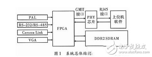
Figure 1 shows the overall structure of the system. In addition to using a DDR2 SDRAM chip, the physical layer function in the network model is performed by a PHY chip. At present, the general PHY chip is compatible with Ethernet transmissions of 10 Mbit·s-1, 100 Mbit·s-1, and 1 000 Mbit·s-13, and provides various interfaces to the upper layer, such as MII, GMII, RGMII, and TBI interfaces. Wait, for the host computer side is directly the ordinary RJ45 network port slot. The physical layer receives the parallel data of the data link layer and converts it into the original bit stream; it also converts the original bit stream into parallel data and submits it to the data link layer.
2 FPGA module function
The FPGA module completes data acquisition, packing, transmission, packet loss and retransmission by responding to instructions from the host computer. The basis of all work is the reliable implementation of the OSI reference model layer protocols such as MAC sublayer, network layer, and transport layer. Each layer provides specific services to the upper layer according to the standard interface, and the details of how to implement these services are the same. The layers are shielded.
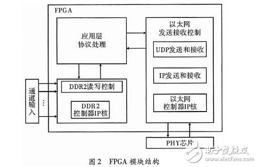
Figure 2 shows the specific structure of the system FPGA module and the relationship between the various submodules. In order to shorten the design cycle and improve the design quality, Altera's existing Ethernet controller IP core and DDR2 controller IP core resources are respectively called in the module.
2.1 DDR2 read and write control
If you do not consider the packet loss in the network, the data is collected while being packaged and sent to the host computer for transmission. It does not require external memory for caching. However, in actual tests, it is found that PCs with common configurations cannot withstand the fast transmission capability of Gigabit Ethernet, and packet loss is very common. Especially when adding to multiple channels, the output capacity of the device to the upper computer is increased, and packet loss is caused. The rate also immediately increased. Therefore, it is necessary to use a piece of DDR2 SDRAM to buffer the data of each channel.
In the design, the DDR2 SDRAM controller provided by Altera Corporation is directly called, and a chip that it can drive is selected to improve the work efficiency. The cache space that the chip can use is a major concern. Each channel must be assigned a fixed buffer area, so the limited memory space should be reasonably divided. In the case of image data, a single channel must have at least two or more frames of space. The DDR2 read/write control module directly calls the IP core of the DDR2 SDRAM controller. However, since the interface provided by the IP core to the client is inconvenient to use, it is necessary to perform burst read and write according to the timing described in the document.
The function of this module is mainly to coordinate the writing and reading of the collected data of each channel. As shown in FIG. 3, during the write operation, the data of each channel is first cached by the FPGA resource, and then the write control state machine sequentially checks the amount of data that has been buffered by each channel by polling, if enough burst writes, Write it into the corresponding channel block of the SDRAM chip, and then check the next channel; during the read operation, the read control state machine also checks the amount of data written to the SDRAM chip by each channel in turn, if there is enough burst read, It is read out and sent out over the network.
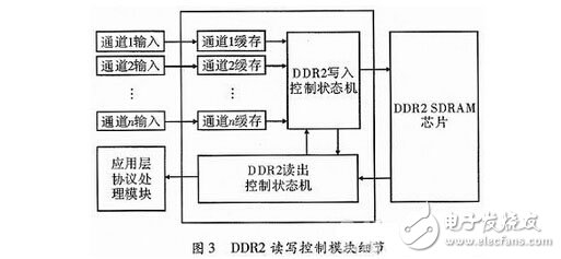
Based on the above control methods, the data format of each channel is not limited. As shown in FIG. 1 , it may be an image or a combination of various formats such as PAL, Camera Link, VGA, etc., but the respective channels are reported to the upper computer before the acquisition. Data information. However, it should be noted that the sum of the bandwidth of these data should theoretically not exceed the maximum transmission rate of Gigabit Ethernet, which is a prerequisite for successful polling. In fact, the processing power of ordinary PCs is far from reaching this maximum limit. When the speed reaches 100 Mbit·s-1, the packet loss of the host computer is already very serious. If the collected data is displayed on the host computer, it may only be 70~80 Mbit·s-1; if the data is to be written to the hard disk, the data rate will be lower, except that a good hard disk is provided. Also need to work harder on the optimization of the PC software.
2.2 Ethernet transmission and reception control
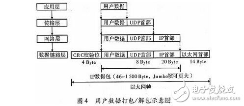
The function of this module is the specific implementation of the MAC sublayer, network layer, and transport layer layer protocols. These submodules, as channels for data transmission, need to have certain caching and error checking capabilities, and must be maintained in order to extend other protocols. Independence between each other. As shown in FIG. 4, the process of receiving data by the hardware device is that the Ethernet frame passes through each layer, removes the header of each layer and checks the verification, and finally obtains pure user data; the process of transmitting data is that each layer of user data passes through, Add the appropriate headers and checksums until a complete Ethernet frame is formed.
1) The function of the MAC sublayer. The design calls the Altera Corporation's three-speed Ethernet controller IP core to implement the MAC sublayer function. The IP core provides a unified register interface, which allows users to configure the Ethernet maximum frame length, source MAC address, and destination. Important information such as MAC address and PHY address. As shown in Figure 4, when transmitting data, the MAC module adds an Ethernet header to the data frame and adds a 32-bit check code using the CRC algorithm. When receiving data, the MAC module also performs a CRC check for incorrect data. Frames should be discarded, and the user can also use the configuration register to determine whether to send the check bits to the previous layer.
(2) Implementation of the UDP/IP protocol stack. Compared with the three-way handshake of the TCP protocol, the UDP and IP protocols are oriented to the connectionless nature so that they can be implemented quickly on the hardware. As for the establishment of the connection, it can be implemented at the application layer.
As shown in Figure 4, the functions of UDP and IP protocols have more similarities in hardware implementation: for the data sent by the upper layer, the corresponding header and checksum need to be added; for the data received by the lower layer, checksum is checked. And remove the header before it can be sent to the upper layer; because there is a length area of ​​the packet in the header, both the sending and receiving, the data packet needs to be fully cached to determine its length, which is equivalent to a kind of " The mechanism of store-and-forward.
Of course, the UDP protocol and the IP protocol also have different places in implementation, mainly reflected in the calculation method of the checksum. The checksum of the UDP protocol is to check the header and the data together, and this header is not only a UDP header of 8 Bytes, but also a pseudo-header of 12 bytes. The calculation of the checksum at the UDP layer also uses the address of the IP layer, but this is contrary to the concept of the network layering model. The checksum of the IP protocol only calculates the header of the IP packet. In general, there is only a fixed 20 Byte.
2.3 Application Layer Protocol Processing
The data collected by different channels is packed according to the specified packet length, and then sent to the above Ethernet control module. Special modules are needed for organization and scheduling, and the corresponding channel labels are added. At the same time, the network does not only collect data packets from the device to the host computer direction, but also has a reverse command packet for control: The first question to consider is when the device starts collecting data and when to stop collecting. It is necessary to send commands to the host computer to control; secondly, for the statistics and processing of lost packets, this part of the work is somewhat difficult, but both the device and the host computer can be completed, obviously it is more appropriate to handle the upper computer, then the upper computer The device sends a short data packet with the missing packet sequence number, and the device preferentially finds the lost data packet from the DDR2 cache and sends it to the upper computer.
The modules that perform these functions in the system are equivalent to an application layer protocol located above the UDP/IP layer. The content of this protocol is specified by the system designer, but must be used by the FPGA developer and the host software program developer. Sharing, so that there is a peer (Peer) that can communicate with each other on the corresponding layer on different machines. In this way, the application layer protocol is developed, which not only increases the confidentiality of the system-related functions, but also allows the developer to tailor the application layer functions, flexibly coordinate the details that the software and hardware should be responsible for, and finally finalize the most compact implementation.
3 PC software features
Since the hardware part of the system implements the content of the UDP/IP protocol stack, the host computer software has more available system calls during development, mainly the use of Socket (socket) primitives. Compared with hardware development, software development is convenient to implement some complex functions and calculations. Therefore, at the beginning of the system conception, some hard-to-implement parts are deliberately handled by the host computer software, mainly the identification and weight of image frame interval. The statistics of the subcontracting.
Regarding data packet retransmission, when transmitting the images of each channel, the hardware device only selects a suitable point to start collecting images, and is not responsible for adding information such as the start and end of the image frame in the data packet, because this not only deviates from the multi-channel. The original intention of image and data compatibility, and the difficulty of the implementation of the FPGA program, especially the data collected into and out of the DDR2 SDRAM cache, if you add additional flag data in these pure data, may disrupt the layout of the entire buffer. Therefore, the host computer can only judge the interval between image frames according to the amount of data received, and then perform frame-by-frame calculation regardless of display or storage.
4 system design considerations
4.1 Response and suppression of ARP packets
Before sending the UDP packet to the device, the host computer may send an ARP packet to request the MAC address of the device. Therefore, in the FPGA program, it is necessary to be able to respond to the data packet and send an ARP reply, otherwise the device and the host computer will not be able to communicate. After the MAC address of the device is obtained, the upper-layer device temporarily saves it and creates an ARP entry. After the ARP table ages, the ARP request is sent to the device again.
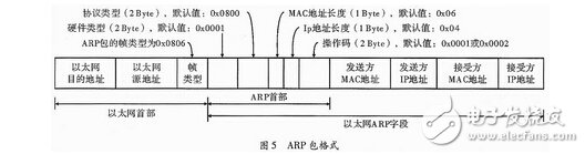
In order to properly respond to ARP requests and replies, the format of the ARP packet must be clear. As shown in FIG. 5, if the value of the "frame type" area of ​​the Ethernet frame is 0x0806, it means that the data behind the frame is filled with an ARP packet. Whether it is an ARP request or an ARP reply, it needs to be identified according to the operation code of the ARP header: the operation code is 0x0001, which is the ARP request packet; and the operation code is 0x0002, which is the ARP reply packet. The ARP request packet fills in a broadcast frame and sends it to all hosts in the network, so its Ethernet destination address is broadcast frame address 0xffffffffffff, and since its destination is to request the destination host's MAC address, the "receiver MAC address" in the figure. The area has no exact value and can be any 6 Byte padding; the ARP reply packet has already obtained the required MAC address, but it should be noted that the sender and the receiver have already been swapped, and the corresponding area should be changed as appropriate.
The shortest frame length specified by the Ethernet protocol is 64 Bytes, which requires that the data padding is at least 46 Bytes, as shown in Figure 4, and the ARP field in Figure 5 has 28 Bytes, so both ARP requests and replies should have 18 Byte padding data. Some PCs send ARP requests from other devices, even if there is only one direct connection to connect the device to the host computer. At this time, the device cannot respond to the request, and such a request should be shielded between the MAC layer and the IP layer to prevent interference with normal packet transmission.
4.2 Pros and cons of Jumbo frames
The maximum frame length specified by the Ethernet standard is 1 518 Bytes, which includes the headers added by the IP layer and the UDP layer. Generally, the packets sent should also be limited to this range. However, Gigabit Ethernet has a vendor-standard ultra-long frame format, which has not yet been approved by the IEEE Standards Committee. It specifies the same frame format as a normal Ethernet frame, except that its data padding area can break through the original limit. The length ranges from 9 000 to 64 000 Bytes, that is, Jumbo jumbo frames.
The advantages of using Jumbo frames in this system: (1) The utilization of network bandwidth can be appropriately increased. This is mainly achieved by saving the addition of the headers of each layer. (2) Reducing the excessive occupation of CPU resources caused by frequent interruptions of the operating system by the operating system. This can be said to be the main reason for using Jumbo frames, because to deal with the higher data rate of Gigabit Ethernet, no matter how the PC software is optimized, the CPU usage is still very high, then if you can reduce the CPU overhead elsewhere, Significantly increase the processing power of the software.
But Jumbo frames also have some disadvantages when used. First of all, many PC network adapters currently do not support Jumbo frame transmission. Although Altera's Ethernet controller IP core supports it, this is not enough for two devices to communicate. Secondly, Jumbo frames will occupy network channels for a long time. It will affect those devices and applications that are sensitive to data delay. Third, packet loss of Jumbo frames means a serious disaster. One frame is equivalent to more than ten normal frames, which will quickly introduce a PC with weak processing capability into retransmission. Trap, more and more packets are lost, until the network bandwidth is fully occupied, causing the PC software to crash. So before considering supporting Jumbo frames, you should fully weigh these advantages and disadvantages.
5 Conclusion
The system hardware device cooperates with the host computer software to complete the data collection task of the dual-channel color PAL system. Through actual testing and analysis, Jumbo frames are used for transmission, which effectively reduces the number of system interruptions during software operation, thereby minimizing CPU usage. Similar high-speed data transfer applications can be extended with the built-in Gigabit Ethernet operating environment.
Tubular Motors for Roller Blind, Venetian Blind, etc.
Tubular Motors
Home Automation Control Motors,Multiple Limits Setting Motors,Quiet Tubular Drive,Tubular Motors
GUANGDONG A-OK TECHNOLOGY GRAND DEVELOPMENT CO.,LTD. , https://www.a-okmotor.com