introduction
At present, digital video coding has become the core and the most basic technical means in video surveillance, video conferencing, network streaming, etc. Especially video surveillance has become one of the most common security equipment. Digital DVRs based on computer hard disks as storage have gradually replaced analog DVRs. The most critical technology of digital DVR is video compression technology, and video compression technology contains two major options. The first is what algorithm standard is used for video compression. The current international standards for video algorithms include MPEG2, MPEG4, and H.264. With its high compression efficiency and excellent image quality at low bit rates, H.264 has become the first choice in current video surveillance systems. Compression method.
But everything has its two sides, the high efficiency of H.264 encoding, and high-quality images are exchanged for the complexity of the algorithm. The complexity of the H.264 encoder is 4-5 times that of MPEG2. The second option is to use what chip to implement. TI's TMS320DM642 chip is a high-speed DSP specially used for media processing. Its powerful image processing capability provides the possibility of real-time H.264 encoding in the monitoring system. In order to reduce costs, it is also necessary to make full use of the resources of DM642, so that a DM642 can process more channels of video, which is the purpose of high efficiency optimization. This article first introduces the entire video surveillance hardware platform, and then combines DM642's Structural characteristics, the arrangement of the entire coding software framework is proposed, and the DSP-based optimization method is proposed for the motion estimation that occupies the most system resources. Finally, the integer DCT is used as an example to discuss the skills of writing assembly code.
Introduction of hardware platform
The framework of the entire video surveillance hardware system is shown in Figure 1. In order to meet the demands of digital media processing, the DM642 chip has added three configurable video ports (VP0, VP1, and VP2). These video ports provide seamless interfaces for common codec devices. Therefore, the system design requirements can be met without the need for external programmable logic devices and FIFO.
In order to save costs and improve the utilization rate of the DSP chip, multiple audio and video can be processed on one board at the same time. The data throughput between the compression card and the host will be very large. In order to ensure the real-time nature of data storage, the system uses PCI boards The data transmission rate of the communication with the host is up to 528MB / s (66MHz, 64bit), which fully meets the needs of high-capacity high-speed real-time transmission system.
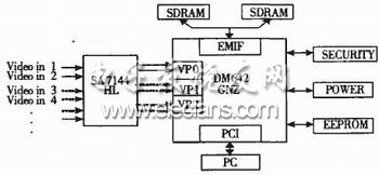
Figure 1 Hardware system framework
Since each video port can receive two 8 / 10bit video signals, the video signal is converted into 8-bit BT.656 format digital video data through SAA7144A / D conversion. In this way, a DM642 chip can be used to process up to 6 video inputs. The BT.656 video capture mode of each video port collects 8-bit or 10-bit 4: 2: 2 format brightness and chrominance signals, and multiplexes them into a data stream. The video data is Cb, Y, Cr, Y, Cb, Y, Cr are transmitted in sequence, where Cb, Y, Cr represent the brightness and chrominance samples at the same position, and Y immediately after represents the brightness samples at the next position. After the data stream is demultiplexed, the luminance and chrominance information are stored in their respective Y, Cb, CrFIFO, and then moved to SDRAM through EDMA, so that the CPU can read it for compression coding. The encoded video stream is then stored on the hard disk of the computer via the PCI port, thereby completing the entire video monitoring process.
Encoder overall frame arrangement
The JM code is one of many optional H.264 standard software. It cares that all the functions of H.264 are reflected in the code. All situations must be considered, such as frame encoding and field encoding, and memory allocation is not considered. To the actual situation of the system, it is suitable for helping to understand the H.264 standard, and is not suitable for porting to the DSP platform. In order to efficiently use the limited on-chip resources of DM642, the code must be reorganized, including the data structure, the location of the data storage, and the location of the program, and the program should be arranged in a streamlined manner.
The first thing to consider is the configuration of L2. The second level L2 (256kB) is a unified program / data space, which can be mapped to the storage space as an SRAM as a whole, or as a second level cache, or a ratio of the two. Use in combination. Because once the second-level cache is not hit, the read data request will be transferred to EDMA to complete, the CPU has at least 13 cycles of delay. So we always try to put the program and data in the on-chip memory. But even if all the L2 is configured as SRAM, it is only 256kB. Taking the CIF format image as an example, the size of the image to be encoded is 148.5kB, and the reference image for motion estimation greatly exceeds 256kB. So when configuring L2, I chose SRAM224kB and L2cache32kB. The first thing to consider is the table, global variables, stack data and some core programs that are called frequently, such as motion search, DCT transform, quantization ... and the entire image to be encoded and the reference image can only be placed in the off-chip storage space Too.
Since the image data is stored in the off-chip storage space, it involves data movement between on-chip storage and off-chip storage. This can be done by the powerful EDMA engine of DM642. EDMA does not occupy CPU cycles during work , Freeing the CPU from the heavy work of moving data, dedicated to computing. When coding the program, in order to avoid the CPU waiting for the EDMA to complete the data before it can work, a double buffer area with a ping-pong structure can be used. When EDMA transfers data to one of the storage areas, the CPU processes the other storage area. After both are processed, the ping-pong area is exchanged.
The data that needs to be moved by EDMA includes the macroblock to be encoded, the reference macroblocks corresponding to the front and rear frames, and the reconstructed macroblock after encoding (not needed for B frame). These macroblocks include the luma block and the chroma block. EDMA can only maximize its performance when moving a large amount of data. If a ping-pong buffer exchange is performed after each macroblock is compiled, it takes too many CPU cycles to frequently configure EDMA channel parameters. The limited on-chip storage space restricts the ability to move too many macroblocks at a time. Generally, it is appropriate to move 7-9 macroblocks at a time. Since the synchronization information of EDMA is sent by the CPU, we naturally think of QDMA, but QDMA is suitable for single, independent and fast data movement. For this periodic and repetitive movement, there is no advantage.
In order to improve the efficiency of EDMA, the EDMA chain can be used to open up to 12 EDMA channels and connect them end-to-end, so that only one trigger of the CPU is needed to convert the luminance block chroma block to be encoded, the luminance block and the chroma block of the reference frame ... Moved once, as shown in Figure 2. When configuring the EDMA channel, we noticed that only the source and destination addresses of EDMA were replaced frequently, while other parameters were unchanged. Since the EDMA controller is based on the RAM structure, each channel is configured through the parameter table. The parameters of each channel can be found in the 2KB configuration table of 0x01A0000h ~ 0x01A07ffh. Therefore, a certain channel is updated. For the source address and destination address of, just write the new address to the configuration table without having to call the corresponding cache function in the CSL library to modify the source address and destination address.
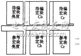
Figure 2 EDMA chain diagram
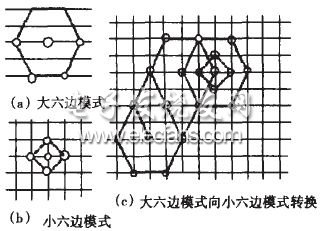
Figure 3 Hexagon search algorithm
There are different type bulbs of parts inside the package. For example, there are one H4 for headlight, one S25 singe filament for signal light, one dual filament S25 for stop light, one G18.5 for truck light or license plate light, one T10 for interior light or side indicators light and two different types of fuses that can replace the burned fuse. The customers will review what specs their own vehicle have and choose which to buy. Having a spare lamp in the car is like buy a insurance, because every light on the car has its specific purpose, which means any broken bulb might put the driver and others in a very dangerous situation. Highly recommend have one kits in the car.
Auto Assorted Lamp Kits
Auto Assorted Lamp Kits,Markcars Car Accessory Kit,Auto Lamp Headlight,Auto Xenon Lamp
Heshan Jianhao Lighting Industrial Co., Ltd. , https://www.sunclubtw.com