Use analog switches to switch videos
Although digital video is gradually becoming popular, analog video is still used in many applications. This article discusses the standard analog video format and how to switch between analog video sources.
In the past, RS-170 was the standard for black and white images. The video was divided into multiple frames, and the standard frame rate was 30 (US) or 25 (Europe) frames per second. Broadcast television divides each frame into two interlaced fields. As far as North American television is concerned, 1/30 second per frame and interlaced scanning, the display image can reach a line scan rate of 15750 lines per second. By convention, the black level is the most negative image signal, and the sync head level is below the black level. The DC level of each part of the signal is shown in Figure 1. 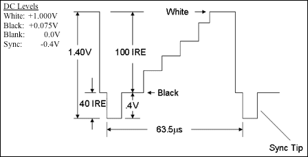
Figure 1. DC level of black and white image signal
The white level to black level of the active part of the video is 100 IRE units, so the white level to the sync head is 140 IRE units. If the signal is attenuated, the ratio of black and white levels and the ratio of white level to sync head will remain unchanged; regardless of whether the signal is attenuated or amplified, the ratio of white level to sync head signal is always 140 IRE units.
Today's composite video baseband signal (CVBS) is a derivative of RS-170, whose white level to sync head has been set to 1.0V (white level +0.714, blank 0V, sync head -0.286). It can be seen as an RS-170 signal that is attenuated by 71%, because all IRE values ​​remain unchanged. The National Television System Committee (NTSC) format modified part of the line width and field width, and very cleverly added the chroma information of the reduced bandwidth to the substantially same baseband signal. Because black and white video signals have been used for broadcasting in the past, (for compatibility with earlier devices), black and white signals are still an integral part of any color television signal system. This information is also called Y, or brightness information. Y is synthesized from all RGB signals¹.
NTSC and later PAL and SECAM have adopted similar methods. Since the Y signal has been used for broadcasting, we need RY and BY signals to generate RGB signals. With the help of the following simple algebra operation, RGB can be extracted from the component signal:
Y = R + G + B, R = Y + (R-Y), G = Y + (G -Y), G = Y-R-B
These operations can be achieved through the sum and difference operations of some simple circuits. For NTSC and PAL, the RY (U) and BY (V) information is modulated so that it can be easily recovered from the baseband signal. For example, when looking at a color NTSC baseband signal output from a DVD player, the signal looks very much like an RS-170 signal. However, we can see that there are many color burst signals similar to "cyclic ringing" on the trailing edge of the sync head, and the frequency is about 3.58MHz / 4.43MHz. The PAL signal also looks very similar, except that the frequency of the H and V sync and color burst signals are slightly different. The nominal value from white level to sync head is 1.0V.
Generally, the rated impedance of a video cable is 75Ω. RG-59 / RG-6 is a standard cable for connecting video equipment, usually equipped with RCA composite video connectors. In Europe, CVBS uses SCART connectors, which integrate CVBS and audio signals.
The CVBS signal bandwidth of all standards is lower than 6.5MHz. Due to the low input impedance and limited bandwidth, most analog CMOS switches today can easily handle this task. This signal contains a negative level part, the designer can use capacitive coupling, and then clamp the signal at the black level. If you are not careful, the sync head may be lost with the color burst signal. Usually the 1.0V signal has a variation range of about ± 6dB, so the signal can be as high as 2.0VP-P, at this time the sync head voltage is about -600mV. Designers can choose an amplifier with a ± 5.0V power supply to bias the switch to prevent problems. If the signal will be transmitted to another CVBS input again, the designer must use a bipolar power supply². If the signal stays on the same circuit board and is used for internal display, then a cheaper biasing scheme can be considered.
Assuming that +5 and -5V power supplies are available, video op amps are almost always required for buffering. The CVBS signal is applied to the non-inverting input of the amplifier. The op amp is usually set to a gain of + 6dB to amplify the signal by 2: 1. Then connect a 75Ω resistor to match the impedance. In most cases, the output is AC-coupled through a capacitor. When a reasonable low-impedance termination resistor is used at the output, the CMOS analog switch performs best. Any capacitor in parallel with the switch is bypassed to ground by the input resistance. Since the CVBS signal must use 75Ω termination resistance, the circuit can be terminated with an impedance slightly higher than 75Ω. If a 300Ω resistor is used as the ground terminal of the non-inverting operational amplifier, then a 95Ω resistor can be used to make the input impedance ideally matched to 75Ω. If the RON value of the analog switch is 35Ω, there will be a slight loss of about 1.0dB. This loss can be compensated by slightly adjusting the gain of the operational amplifier. If the RON value of the switch is higher or lower, the gain can be adjusted accordingly. Because the output of the video operational amplifier is almost zero impedance, its output can also drive other circuits at the same time. It is not advisable to cancel the resistor or use a very high resistance value, as this will cause the video to lose terminal matching, resulting in radiation. Using a 95Ω resistor will not cause any adverse effects, and the circuit can be well terminated. The switch in Figure 2 is a complete circuit for a 2: 1 video switch with a video buffer. The design uses a ± V bipolar power supply design. 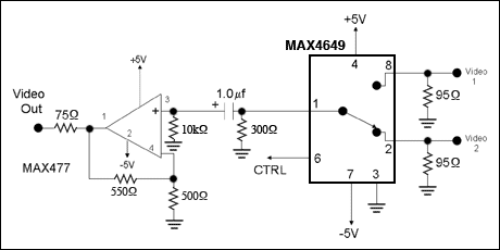
Figure 2. Simple 2: 1 CVBS video switch
CVBS performs well in some applications, but the higher bandwidth recordings that DVDs and other devices can provide raise the demand for higher bandwidth connections.
The S terminal, which mainly appears on some Hi-8 video projectors and DVD players, produces higher bandwidth images by transmitting two (luminance and chrominance) signals. Each signal is transmitted through a special DIN connector. The luminance signal is a broadband version of the composite signal, but does not contain color information. The chrominance signal is the encoded RY and BY signals. Since the bandwidth of the luminance signal is higher now, and there is no need to use a special filter to separate the two signals, a better video signal can be transmitted. Both the luminance and chrominance signals can be transmitted using standard video technology, and the bandwidth of the luminance signal can be increased to about 10 MHz. The circuit type in Figure 2 can be used for dual-channel S-terminal video switching (two sets of switches and buffers).
Component terminals are the latest consumer video interface. Unlike the VGA signal, the component video consists of a Y signal and two color-difference signals (instead of RGB signals). The component video signal has a higher storage efficiency than the RGB signal and is the original signal obtained from the DVD format. The Y signal is full bandwidth and contains synchronization information. The analog signal Y Pr Pb needs to be transmitted from the signal source to the monitor. The following application is a monitor using the new switch MAX4887 with two inputs and a buffered output.
Component video consists of three analog signals: Y, Pr, and Pb, where the Y signal is full bandwidth. The new three-way video switch MAX4887 selected in this application has extremely wide bandwidth and extremely low insertion loss. Similar to the previous application, a single 5V power supply and buffered output are used here, but capacitive coupling is used between the switch and the video op amp. Not only does the bandwidth of the MAX4887 exceed the design requirements, but when the equivalent load is 250Ω, the switching loss is almost zero. In order to pass the low frequency synchronization signal, a 100µf capacitor must be used, and a 0.01µf ceramic capacitor should be connected in parallel to improve the high frequency response. The circuit in Figure 3 shows only one channel. The MAX4887 has three high-frequency switches, so you can use the other two switches to complete the other two input / output circuits to form a complete design. It can also be used without buffer when using MAX4887. 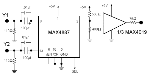
Figure 3. High-bandwidth component video design (only one channel is listed)
The MAX4887 series RON is only 5Ω. The 1kΩ resistor at the input ensures that the input will not float and provides a little return loss matching. The total loss of the switch and matching resistor is 0.6dB. Such small losses usually do not need to be considered. As in the case above, Figure 4 shows only one switch. Both component video and RGB video use three identical circuits, which are included in the MAX4887. 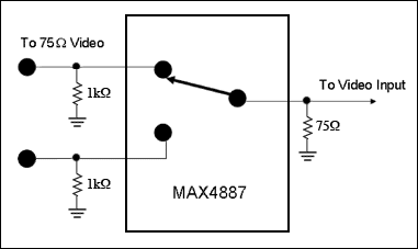
Figure 4. VGA RGB video design using MAX4887
The circuit in Figure 4 is suitable for VGA RGB video. If the video signal has obvious negative peaks, it is not appropriate to use MAX4887 unless the input ESD protection circuit can prevent signal conduction. Otherwise, this situation will occur when the negative polarity signal is lower than -0.3V. If a negative power supply is available, the switch can be operated from + 3.3V to -1.5V. Since the switch hardly needs any current, its negative power rail (usually GND) can be biased to -1.5V, and the switch can still work normally at this time (except for the selection pin). The control level problem can be solved by connecting the emitter of a PNP transistor inverter to + 3.3V and the collector resistor to -1.5V.
Due to the diversity of video signals, there is a need to handle a variety of different video sources. Due to this characteristic of the video signal, a design using a bipolar power supply or capacitive coupling is necessary. Maxim provides a large number of analog switches and video operational amplifiers to easily and economically match these two solutions.
Note:
¹Strictly speaking, RGB should have a scale factor (that is, white = (.30 x R) + (.59 x G + (.11 x B))
² In most cases, the CVBS signal is buffered and output after being received (eg, video input / video output on TV or VCR).
CCTV Power Supply, 4 Channel /9 channel /18 channel 12VDC independent fuse Power Distribution Unit for CCTV camera.
Features:
l Use of efficient, environmental protection switching power supply circuit frame
l Optimization of the shape and structure to facilitate the construction systems
l Small ripple & noise -- video output signal more stable, clearly images.
l Splitter output -- by-pass failure to protect other equipment to work.
l Lower Power Consumption,High reliability.
l Cooling by free air convection ,more stable in quality .
l Power protection -- Output over-voltage protection, over-current protection, short circuit protection.
l 100% full loading burn-in test.
l Warranty: 3 years . and we provide best after sales service .
Product application:
1. Stepping motor
2. PLC control System
3. Surveilance cameras
4. LED advertisement
5. Lamps and lanterns
6. CP communication
7. Communication equipment
8. Industrial control
9. Home Application
10. The traffic and Building


Boxed Power Supply CCTV
Boxed Power Supply CCTV,24V Boxed Power Supply,2 Amp Boxed Power Supply
Guangdong Steady Technology Co.LTD , https://www.steadysmps.com