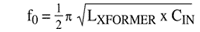
This article discusses a circuit that converts a single-ended signal (usually from a buffered demodulation circuit) into a differential signal (to feed into a high-IF ADC). These circuits use a broadband transformer, matching resistors, and filter capacitors to accomplish this task. The optimal matching method of the transformer is also discussed in order to maintain the high dynamic range of the high-speed ADC while minimizing the effects of gain protrusion and bandwidth reduction. A 200MHz transformer is used to achieve single-ended to differential conversion. We chose the MAX1449 to illustrate and analyze two possible input configurations. Figure 1 shows a typical AC-coupled single-ended-to-differential conversion design using a broadband transformer. The transformer uses Mini-Circuits®'s T1-IT-KK81 (200MHz), which uses 50Ω primary-side matching and 25Ω / 22pF filter network. . In this structure, a single-ended signal from a 50Ω impedance signal source is converted into a differential signal after passing through a transformer. The 50Ω matching on the primary side makes a good match between the signal source and the transformer. But it also means a mismatch between the primary and secondary sides of the transformer. Seen from the primary side is a combined 25Ω impedance, but on the secondary side is a large mismatch impedance, that is, a 20kΩ ADC input resistance in parallel with a 22pF capacitor. This will affect the frequency response of the input network and will ultimately affect the frequency response of the converter. The nominal leakage inductance of the transformer is in the range of 25nH to 100nH. Adding 22pF input filter capacitor will produce an interference resonance frequency between 110MHz and 215MHz
Around this frequency, an annoying gain protrusion will occur.
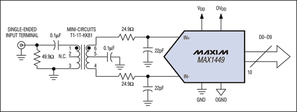
Figure 1. Using a 200MHz transformer to convert a single-ended signal from a 50Ω signal source to a differential signal. Use 800MHz transformer to achieve single-ended to differential conversion. Figure 2 shows an AC coupling configuration similar to Figure 1, but this time a better performance broadband transformer is used, such as Mini-Circuits ’ADT1-1WT (800MHz). Adopt primary side matching and 25Ω / 10pF filter network. Although this transformer has an impedance of 75Ω, its lower leakage inductance can obtain a better frequency response, with a frequency of -1dB up to 400MHz, compared with 50MHz for T1-IT-KK81.
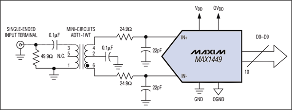
Figure 2. Similar to Figure 1, a transformer is used to convert a single-ended signal to a differential signal, but this time an 800MHz transformer is used, so it can provide better performance. Transformer-200MHz vs. 800MHz Figure 3 shows the test results of two matching schemes, filter network components and transformer. It can be seen from the two curves in the figure that the frequency response characteristics are significantly improved. The T1-IT-KK81 transformer clearly exhibits a gain bump of approximately 0.5dB between 90MHz and 110MHz, while the curve of the ADT1-1WT transformer remains flat within 0.1dB in the frequency range up to 300MHz. The dynamic performance under this condition (ie, ADT1-1WT transformer, 50Ω primary-side matching, and 10pF input filter capacitor connected to INP and INN) can still achieve a SNR of 58.4dB at a frequency of fIN = 50MHz. Although only the 80MHz to 260MHz test frequency is shown in Figure 3 (ADT1-1WT transformer only), laboratory test results have shown that even when the input frequency is far beyond the 8th Nyquist zone, its gain flatness It can still be kept within 0.1dB.
Figure 3. The gain flatness obtained with an 800MHz transformer is much better than the gain flatness obtained with a 200MHz transformer.
Matching the impedance of the secondary side of the transformer helps to further improve the gain flatness. One method is to match on the secondary side of the transformer instead of the primary side.
Especially for high and intermediate frequency applications, the location of the matching impedance is critical. According to different requirements for gain flatness and dynamic performance, the AC-coupled input signal can be matched on either side of the transformer. A broadband transformer is a common device that can quickly and easily convert single-ended signals into differential signals over a wider frequency band. For primary-side matching, we chose MAX1124 (10-bit, 250Msps) to illustrate different matching schemes and their impact on ADC gain bandwidth and dynamic range. We start with the primary-side matching structure (Figure 4a) and connect two of a 50Ω impedance to the 25Ω resistors between the top / bottom of the transformer and the center tap (Figure 5a). It is followed by a 0.1µF AC coupling capacitor and input filter network (15Ω series resistance and ADC input impedance). Now, what is fed into the converter will be a well-balanced secondary side signal. As in the configuration in Figure 4a, no other input filter capacitors are connected to INP and INN. With this configuration, gain bumps in the frequency range of 450MHz to 550MHz can be almost completely eliminated. If necessary, more DC attenuation can be added by replacing the 15Ω isolation resistance with 30Ω. Although this method can make the frequency response flatter, it also loses some bandwidth (Figure 5b).
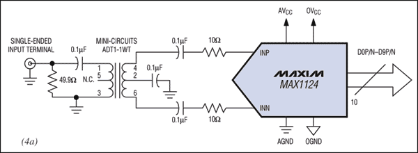
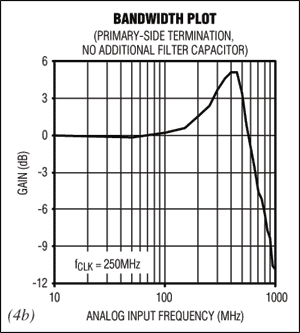
Figure 4. In this primary-side matching structure (Figure 4a), the good balance on the primary side of the transformer is destroyed by the imbalance on the secondary side, resulting in a maximum gain bump between 450MHz and 550MHz (Figure 4b).
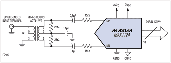

Figure 5. Feeding a well-balanced secondary-side signal into the converter (Figure 5a) completely eliminates the gain bump in the 450MHz to 550MHz range. At the same time, DC attenuation can be increased to make the frequency response flatter, but this will lose some bandwidth (Figure 5b). Conclusion The discussion in this article shows that the correct selection of passive devices not only plays an important role in the design of the input network of high-speed analog-to-digital converters, but also the correct use of these devices. For example, if gain flatness is an important factor in system design, care must be taken to avoid imbalance and resonance on the differential input of the converter to ensure true reproduction of its dynamic performance. The two structures that do not use input filter capacitors may have INP and INN pick-up noise concerns. A simple analysis of this problem indicates that this will result in a 0.2-0.5 dB reduction in signal-to-noise ratio (SNR). When focusing on high bandwidth, gain stability (flatness) over a wide frequency range, and high dynamic performance, most high-IF applications that use 10-bit data converters can accept such small noise performance degradation.
Smart solar outdoor light with both lighting and RGB colorful lighting, can be charged with USB and solar panel. Once it has sunlight, the solar panel can be automatically charged , the charging way is very environmentally friendly. We added a USB charging way so that it can be quickly charged via the USB cable in cloudy day or rainy day.
The outdoor light is solar-sensing, it will automatically turns off when in the bright enviroment, then begin to charge by solar. When the night comes, it will automatically turn on in the dark. Waterproof IP65 makes users no need to worry when using in the rainy day.
Equipped with a detachable plastic sticker, it can be used to decorate the lawn, garden, beach... After removing the plastic sticker, it can be placed on the table as an ambient light. They will be stars fall into your garden, twinkle in the dark and go off in the day. Automatic cycle colorful mode makes parties begin at anytime and anywhere.

Our LED products can meet global quality standards and pass European testing by TUV Rheinland. Bulbs have certifications such as EMC, RED, LVD, ROHS, REACH, ERP and FCC.
The App are developed on the most advanced Bluetooth Mesh technology. [LinkupHome" App can be downloaded in the App store or Google Player, then you can control our product without any complicate steps. The App is stable, easy control and multifunctional.


The advantages of Bluetooth Mesh are fast connect, low power consumption, no password required and Ad-Hoc Network. No need WIFI and hubs, as long as you have a Bluetooth-enabled smart phone, you can experience the smart light. When you install several smart solar lamps, the self-organizing network function can make the signals free connect, break the limitation of distance.
Product Parameters
Description: Bluetooth Mesh RGB Outdoor Solar Lamp with APP
Bluetooth: CSR Bluetooth Mesh
Control Qty: 1-48pcs
Control distance: 20m
Product dimension: 155mm *235mm
Material: ABS+PC
Lamp Color: 8pcs RGB lamp beads+4pcs Warm White lamp beads
Lamp Current: 15-20mA
LED Power: 0.4W(15LM)
Battery Capacity: 3.7V, 1000mA Li-battery included
Charge Mode: Solar panel and a USB
Battery Using time: 9h(by USB charge for 1.5h) , 5h(by solar panel for whole sunny day)
Solar Panel: Monocrystalline silicon
Solar Panel Voltage: 6V
Solar Panel Output: 130mA
Waterproof Level: IP65
Warranty time: 1 Year
Certification: CE(EMC,RED) ROHS,IP65,FCC
Color box size: 22.2*20.6*5cm
G.W. of Unit: 0.55kg
N.W. of Unit: 0.34kg
Outdoor Lamp With APP,Smart Outdoor Lighting System,Phone Control Outdoor Lamp,APP Control Outdoor Lamp
Ningbo Homey Photoelectric Technology. Co., Ltd , https://www.linkuphome.com