Abstract: This application note helps system designers to select the correct external components when using the MAX16948 dual-channel remote antenna LDO / switch to ensure that the vehicle regulated phantom antenna power supply and output current monitoring circuit meet performance specifications. This article provides an electronic calculator to help define the critical external components of the MAX16948 and reduce design time. The calculator also determines the device's analog output voltage, output current-limit threshold, and output current detection accuracy. The calculator includes a new automatic step-by-step wizard function to help designers select components. To use the new automatic function, click the Step By Step button in the corresponding section.
introduction
The MAX16948 is a dual-channel, high-voltage, low-dropout linear regulator (LDO) / switch with output current detection. The device provides phantom power to remote radio frequency (RF) low noise amplifiers (LNAs) in automotive systems via coaxial cables, with a maximum current of 300mA per channel. The MAX16948 is designed to operate from an input voltage range of 4.5V to 28V (45V load dump tolerance).
The device provides a fixed regulated output voltage of 8.5V or an adjustable regulated output voltage from 1V to 12V (LDO mode). The device can also be configured as a switch (SW mode).
The MAX16948 monitors the load current of each channel and provides two analog output currents (sourced from the SENSE_¹ pin) that are proportional to the detected output current. The high-precision internal adjustable current limit protects the input power supply from damage from overcurrent and short circuit conditions.
The device has battery short-circuit protection, reverse current detection, input overvoltage and thermal overload shutdown. During these fault conditions, the internal LDO / switch is blocked. The MAX16948 includes two independent low-level active, high-voltage compatible shutdown inputs (SHDN_) that can put each channel into a low-power shutdown mode and two low-level open-drain error alarm outputs (ERR_).
MAX16948 external components
Figure 1 shows the typical application circuit of MAX16948. The main external components and their functions are as follows:
R1_ and R2_ set the regulated output voltage when the device is in LDO mode with adjustable output voltage. RLIM_ sets the current limit threshold. RSENSE determines the ADC full-scale input voltage and output current detection accuracy.
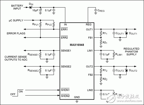
Figure 1. Typical application circuit of MAX16948.
Using these external components, users can easily configure the MAX16948 for specific applications. Other external components are needed, which will be discussed below.
Input capacitance
Connect electrolytic capacitors and low ESR ceramic capacitors in parallel between IN and GND to limit the input voltage drop during transient output short-circuit conditions and protect the device from transient damage caused by inductance on the IN line. For example, if the input inductance (including any stray inductance) is estimated to be 20µH, use at least 0.1µF ceramic capacitor in parallel with at least 10µF electrolytic capacitor.
When the operating input voltage of the MAX16948 is close to the output voltage, such as the SW operating mode or LDO mode under a differential pressure, care must be taken to avoid erroneous reverse current detection during a short-to-ground fault. If both channels are enabled and one of them is shorted to ground after startup, the current drawn from CIN may cause the input voltage to drop for a short time, which may trigger a reverse current detection fault. This kind of false fault detection is more serious at low output current (less than 80mA). To avoid this false triggering event, use an input electrolytic capacitor of at least 100µF.
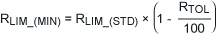
LDO mode output voltage
When used in LDO mode, each channel of the device can be configured to provide a fixed output of 8.5V or an adjustable output voltage from 1V to 12V. By connecting the FB_ pin to REG, the output voltage is set to 8.5V. In this mode, since there is no need to consider the tolerance of the external resistor, the output voltage accuracy is high.
When different output voltages are required, connect a resistor divider between OUT_, FB_ and GND. The formula for determining the value of the resistor divider is shown below.
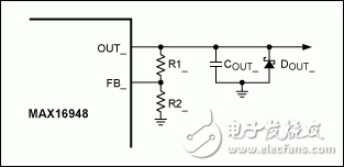
Figure 2. MAX16948 regulated phantom power supply.
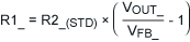
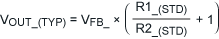
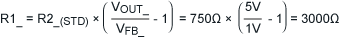
Resistors R1_ and R2_ (Figure 2) set the output voltage of the MAX16948. Choose an R2_ standard resistor (R2_ (STD)) less than or equal to 1kΩ. Use the following formula to calculate the optimal R1_ value:
In the formula, VFB_ is the feedback pin voltage within the adjustment range (the nominal value is 1V).
After selecting the standard resistance as close as possible to R1_²R1_ (STD)), the typical output voltage is:
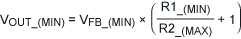
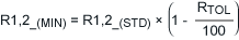
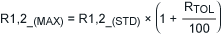
Considering the resistance tolerance (RTOL), the minimum and maximum values ​​of the output voltage are:
and
In the formula, VFB_ (MIN) is 0.97V, VFB_ (MAX) is 1.03V (output current range is 5mA to 150mA). R1_ (MIN), R1_ (MAX), R2_ (MIN) and R2_ (MAX) are the minimum and maximum values ​​of R1_ and R2_, respectively:
If the deviation of the nominal output voltage from the expected output voltage is too large, a series or parallel combination of standard resistors can be used to achieve an optimal resistor divider.
The expected output voltage (VOUT_), the standard values ​​of R2_ and the tolerances of these resistors are filled into the corresponding part of the MAX16948 calculator. The user can easily determine the value of R1_. After the calculator determines the optimal R1_ value, insert the standard value in the corresponding unit to estimate the VOUT_ range limit. Or, click the Step By Step button, and the calculator will gradually guide you through the LDO mode output voltage part.
Connect a capacitor> 1µF between OUT_ and GND in parallel with a 0.1µF low ESR (<900mΩ) capacitor to achieve regulator stability. These capacitors should be as close as possible to the device. Use a capacitor with a dielectric of X7R to ensure stability over the entire operating temperature range of the device.
Similar to the input capacitor, the output capacitor protects the device from transient damage caused by any series inductance in the output. Under any conditions, the voltage on OUT_ should not be lower than -0.3V, as specified in the Absolute Maximum RaTIngs section of the data sheet. If the transient is expected to be lower than ground, a Schottky diode is required for clamping, especially if there is an output inductor on the PCB before the load. The forward bias of the selected Schottky diode must be less than 0.3V, and the forward current is equal to the current limit threshold. ³
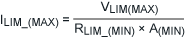
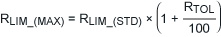
Current limit threshold
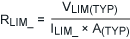
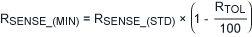
When the voltage at the LIM_ pin reaches the VLIM threshold (typically 2.5V), the MAX16948 limits the output current of OUT_. The current from the LIM_ source is proportional to the load current from the OUT_ source, and the scale factor is called the current sense amplifier (CSA) gain. In this way, the current limit threshold ILIM_ is set by the resistor RLIM_.
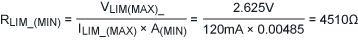
Use the following formula to determine the optimal RLIM_ value:
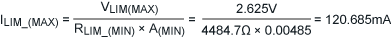
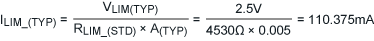
In the formula, ILIM_ is the expected current limit threshold, VLIM (TYP) is the typical voltage threshold (2.5V) on the LIM_ pin when limiting the output current, and A (TYP) is the typical value of the CSA gain (0.005mA / mA).
Select the standard resistance value (RLIM_ (STD)) as close as possible to RLIM_. Then the typical current limit threshold is:
Considering the tolerance uncorrelation, the worst-case current-limit threshold range is between the following two formulas:
and
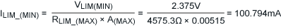
In the type, VLIM_ (MIN) is 2.375V, VLIM_ (MAX) is 2.625V; A (MIN) is 0.00485mA / mA, A (MAX) is 0.00515mA / mA (typical output current 100mA); RLIM_ (MIN) and RLIM_ (MAX) is the minimum and maximum value of RLIM_, based on the value of RTOL.
If the current limiting threshold range is not suitable, a series or parallel combination of standard resistors can be used to obtain the optimal range.
The MAX16948 calculator 4 calculates the optimal value of RLIM_ by selecting the current-limit threshold range limit (ILIM_ (TYP), ILIM_ (MIN), or ILIM_ (MAX)) to help users select RLIM_ resistance. By selecting ILIM_ (TYP), ILIM_ (MIN) or ILIM_ (MAX), and the relative current limit threshold and RLIM_ tolerance, the above purpose is achieved. After the calculator determines the optimal RLIM_ value, insert the standard resistance value in the corresponding unit to estimate the ILIM_ range limit. Or, click the Step By Step button, and the calculator will gradually guide you through the current limiting threshold.
A 0.1µF compensation capacitor (CLIM__) must be connected in parallel with RLIM_ to establish a dominant pole in the current limiting loop. This maintains stability and prevents rapid current transients from triggering the current limit prematurely (Figure 3).
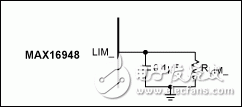
Figure 3. MAX16948 output current limit.
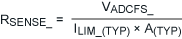
ADC input range and output current detection accuracy
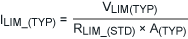
The current sourced by the MAX16948 is proportional to the load current on the OUT_ pin, and the scale factor is the CSA gain. This current passes through RSENSE_, producing a voltage proportional to the output current. Using this feature, it is possible to use the ADC to sample the voltage on the SENSE_ pin to monitor the output current.
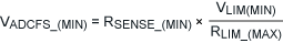
The ADC full-scale input voltage (VADCFS_) is set by RSENSE_.
Use the following formula to determine the optimal RSENSE_ value:
In the formula, ILIM_ (TYP) is the typical current-limit threshold calculated in the previous section, and A (TYP) is the typical value of CSA gain (0.005mA / mA).
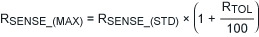
Select the standard resistance value (RSENSE_ (STD)) as close to RSENSE_ as possible. Then the typical ADC full-scale input voltage is:
Taking into account the resistance tolerance (RTOL), the minimum and maximum values ​​of the ADC full-scale input range are:
and
In the formula, VLIM_ (MIN) is 2.375V and VLIM_ (MAX) is 2.625V; RLIM_ (MIN) and RLIM_ (MAX) have been calculated in the previous part; the minimum and maximum values ​​of RSENSE_ (MIN) and RSENSE_ (MAX) Based on RTOL value.
Using the output current detection part of the electronic calculator 5, the user can easily determine the value of RSENSE_ after inserting the tolerance of the corresponding ADC full-scale input voltage (VADCFS_) and RSENSE_. After the calculator determines the optimal RSENSE_ value, insert the standard value in the corresponding unit to estimate the VADCFS_ range limit. Or, click the Step By Step button, and the calculator will gradually guide you through the output current detection part.
However, before using this part, the ILIM_range limit needs to be determined in the current limit threshold part of the calculator.
A 0.1µF capacitor (CSENSE) should be connected in parallel with RSENSE_ to maintain the voltage during the ADC sampling cycle (Figure 4).
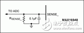
Figure 4. ADC input range.
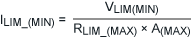
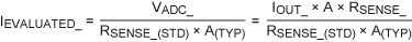
After measuring the voltage on the SENSE_ pin using the ADC (VADC_), the output current can be estimated using the following formula:
Due to the discrete RSENSE_ tolerance and CSA gain parameter values, the estimated output current value will vary between the following two formulas:
and
Replace the CSA gain value with a typical output current of 100mA:
Finally, the accuracy of the ADC's current measurement is:
This parameter can also be determined in the OCS accuracy line of the output current detection section of the calculator.
Load open circuit and over current condition detection
In addition to ADC sampling, by using an external comparator and dividing RSENSE_ into resistor dividers (R3_, R4_, and R5_) (Figure 5), open load or overcurrent conditions can be detected.
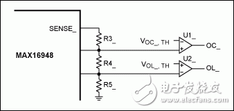
Figure 5. Open load and overcurrent detection circuit.
The output of the comparator (OC_ and OL_) represents the working state of the circuit, as shown in Table 1.
| Table 1. Circuit operating status |
| OC | OL | State |
| 0 | 0 | Normal OperaTIon |
| 0 | 1 | Open-Load CondiTIon |
| 1 | 0 | Overcurrent CondiTIon |
| 1 | 1 | Invalid State |
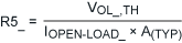
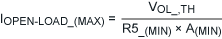
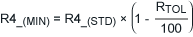
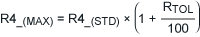
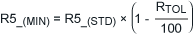
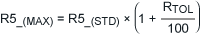
Determine the R5_ value using the following formula:
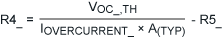
In the type, IOPEN-LOAD_ is the expected load open current threshold through the LDO / switch, VOL_, TH is the load open circuit voltage threshold of comparator U2_, and A (TYP) is the typical value of CSA gain (0.005mA / mA). After calculating the R5_ resistance value, use the following formula to determine the R4_ value:
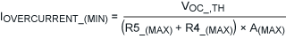
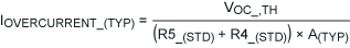
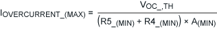
In the formula, IOVERCURRENT_ is the expected overcurrent threshold through the LDO / switch, which must be less than ILIM_ (MIN); VOC_, TH is the overcurrent voltage threshold of comparator U1_; A (TYP) is the typical value of CSA gain (0.005mA / mA).
Finally, calculate R3_:
R3_ = RSENSE_-R4_-R5_
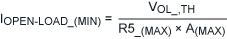
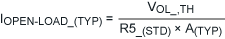
Considering the tolerances (RTOL) of R3_, R4_, and R5_ standard resistors, the minimum, typical, and maximum values ​​of the open load and overcurrent thresholds are:
In the formula, A (MIN) is 0.00485mA / mA, A (MAX) is 0.00515mA / mA (typical output current 100mA); R4_ (MIN), R4_ (MAX), R5_ (MIN) and R5_ (MAX) are respectively The minimum and maximum values ​​of R4_ and R5_ are based on RTOL tolerance.
The user can determine the values ​​of R4_, R5_, and R6_ using the open load and overcurrent detection section of calculator 6. Insert IOPEN-LOAD_ (IOL_), IOVERCURRENT_ (IOC_), VOL_, TH, VOC_, TH and resistance tolerance. After determining the optimal values ​​of R4_, R5_ and R6_ with a calculator, insert standard resistance values ​​in the corresponding units to estimate the range limits of IOPEN-LOAD_ and IOVERCURRENT_. Click the Step By Step button, and the calculator will gradually guide you through the load open circuit and overcurrent detection parts.
Before using the load open circuit and overcurrent detection part of the calculator, you need to determine RSENSE_ in the output current detection part.
Calculation example
In these calculation examples, we assume the application of antenna phantom power, the power input voltage is 5V, the typical load current is 100mA, the maximum current limit threshold is 120mA, and the output current is monitored with a 3.3V input range ADC.
Assuming that the IN pin of the MAX16948 is directly connected to the battery, the device must be configured in LDO mode to obtain a 5V OUT_ voltage. For this, the external resistor divider composed of R1_ and R2_ must be determined. Choose a standard value less than or equal to 1kΩ for R2_ (R2_ (STD)), and then calculate R1_:
R2_ (STD) = 750Ω, RTOL = 1% (E96 Series)
Select the standard resistor (R1_ (STD) = 3010Ω) from the E96 series, the output voltage range is:
To make the maximum current limit threshold (ILIM_ (MAX)) equal to 120mA, the ILIM_ (MAX) formula can be rearranged to calculate RLIM_:
Select the standard resistor (RLIM_ (STD) = 4530Ω) from the E96 series. The current limit threshold range is:
When the ADC input range is 3.3V, calculate the optimal RSENSE_ as follows:
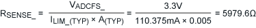
Select the standard resistor from the E96 series (RSENSE_ (STD) = 6040O, RTOL = 1%), the ADC full-scale input voltage range is:
VADCFS_ (TYP) = RSENSE_ (STD) × ILIM_ (TYP) × A (TYP) = 6040Ω × 110.375mA × 0.005 = 3.333V
VADCFS_ (MIN) = RSENSE_ (MIN) × ILIM_ (MIN) × A (MIN) = 5979.6Ω × 100.794mA × 0.00485 = 3.104V
VADCFS_ (MAX) = RSENSE_ (MAX) × ILIM_ (MAX) × A (MAX) = 6100.4Ω × 120.685mA × 0.00515 = 3.571V
Then the accuracy of the output current monitoring is:
Radiation XLPO insulated
Control Cable is not
cross-linked by normal chemical cross-linking material under high temperature
and high pressure, but cross-linked by
high energy electron accelerator or rays. That is why radiation XLPO insulated
control cables get higher
electrical property, excellent
flame retardant property, Stronger
mechanical property, they are also with better resistant to heat-aging,
scratching, abrasion, oil, melting, and environmental stress crack. The most common material
used for radiation cross-link cables are PVC, XLPE.
Product features
Long-term
temperature: Up to 125℃
Conductor: OFC copper
Heat-resistant
level: 90℃,105℃,125℃
Rated voltage: Up to 0.6/1kV


Application
This cable is used
in control system, electrical equipments and instruments, especially suitable for high temperature
and fire retardant condition.
FAQ
Q: Are you a factory or trading company?
A: We are a manufacturer. We are professional in developing
and producing electrical wires and cables since 2001.
Q: Can I visit your
factory?
A:Yes! You are welcome to
visit our factory for further detail check.
Our factory is located in Minqing,Fujian.You could choose to fly
to Xiamen/Fuzhou International airport. And tell us your flight No. We will arrange to pick you up
if you like.
Q: May I buy samples from you?
A: Yes! You are welcome to place sample order to test our superior quality and services.
Q: Can you put my brand name (logo) on these products?
A: Yes! Our factory accepts to print your
logo on the products.
Q: May I know the status of my order?
A: Yes .The order information and photos at different production stage of your order will be sent to you and the information will be updated in time.
To receive a quote, further information or advice, Leen Cable invites you
to contact us.We believe we will become your best partner in electrical cables
and wires services.
Radiation XLPO Insulated Control Cable
Radiation XLPO Insulated Control Cable,Copper Screened Control Cables,Armoured Shielded Control Cables, Shielding XLPE Control Cable
Smartell Technology Co.,Ltd , http://www.liencable.com