Principle and design of analog isolation amplifier circuit using optocoupler
This paper presents a new design scheme for isolation amplifiers, which has a simple structure and uses universal devices, which is easy to implement. The circuit is compared with AD210AN integrated analog isolation amplifier of AD company. The isolation amplifier circuit is better than the integrated analog isolation amplifier in bandwidth.
Isolation amplifier according to the type of transmission signal. Can be divided into analog isolation and switching isolation amplifier. There are fewer manufacturers and product types of analog isolation amplifiers, and the products are more expensive. There are many manufacturers of switching isolation amplifiers, and there are many types of products. The prices are relatively low and relatively cheap. High-priced analog isolation amplifiers limit its scope of application. The dual-channel isolation amplifier mentioned in [2] has a complicated structure. And there are higher requirements for the isolation distance, and the photocoupler isolation amplifier mentioned in [3] has higher requirements for component parameters. The isolation amplifier mentioned in [4] also has special requirements for the separation distance of isolation devices.
1 New circuit principle Figure 1 shows the principle circuit of the isolation amplifier designed by the author. This isolation amplifier circuit is mainly composed of a photocoupler and an operational amplifier. The optocoupler selects the ordinary optocoupler TLP521, and the op amp selects the general op amp LF353. Through the combination of these two common devices, the performance of the isolation amplifier is similar to that of the dedicated analog isolation amplifier.
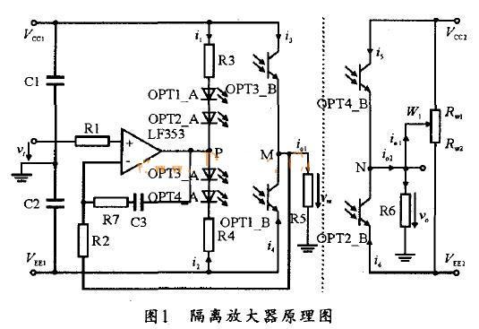
Figure 1 shows an isolated amplifier circuit composed of an amplifier and an ordinary optocoupler. The isolated amplifier circuit is composed of two parts: input and isolated output, and the two parts are powered by isolated power supplies (Vcc1, Vee1 and Vcc2, Vee2. The input part is provided by the operational amplifier U1, resistors R1, R2, R3, R4, R5, and capacitor C1 , C2, OPT1_A, OPT2_A, OPT3_A, OPT4_A and OPT1_B, OPT3_B of OPT1_A, OPT3_A, OPT3_B, OPT3_B of OPT1_A, OPT2_A, OPT3_A, OPT3_B, OPT1_A, T, OPT2_A, T The currents of OPT3_A and OPT4_A form a differential amplifier input. R1 and R2 are the input resistance of the op amp, R3 and R4 can provide bias and control current for the four optocoupler light-emitting diodes (LED). , OPT3 constitutes a shot follower, the voltage on R5 is the input voltage of the op amp.
The bandwidth of the op amp determines the bandwidth of the isolation amplifier. The bandwidths of existing integrated analog isolation amplifiers are all below 100 kHz, and the bandwidth of commonly used op amps is several to tens of times this bandwidth. Therefore, the general op amp used in this design can meet the bandwidth requirements of the input section. Therefore, the op amp of the input stage can use ordinary op amp (such as LF353). R7 and C3 are used for filtering. The isolated output part of this circuit is composed of OPT2, OPT4 phototransistor OPT2_B, OPT4_B, potentiometer W1 and output resistance R6. OPT2_B and OPT4_B are isolated outputs. Its circuit structure is similar to the phototransistor in the input part, and is used to provide current for the output stage. Potentiometer W1 is used for zero adjustment. When the current transfer ratio of the two parts of the optocoupler deviates, it will cause the optocoupler LED current to be equal and the output stage current difference to be different, thereby causing the zero point of the output voltage vo to drift. Therefore, adjusting the potentiometer W1 can eliminate the zero drift caused by the deviation of the characteristics of the optocoupler device. R6 is the output load, which determines the output voltage vo together with the potentiometer W1. It can be seen that the ordinary optocoupler can be used for this design (such as Toshiba's optocoupler TLP521).
2 AD210AN integrated amplifier AD210AN is the integrated analog isolation amplifier chip of AD company. In this isolated amplifier circuit, the two pins 16 and 17 of the AD210 are connected together to realize the signal tracking function. The signal source Vs is connected between the two pins 18 and 19 through the resistor Ra, and the 18 pin and Vs share the ground. Pin 1 and pin 2 are output pins, and Rb is the output load resistance (Ra = Rb = 1 kΩ can be selected when using). This circuit can realize 1: 1 isolation transmission function.
3 Experimental verification In testing this circuit, select Vcc1 = Vcc2 = 12V, Vee1 = Vee2 = -12 V, R1 = R2 = 18 kΩ, R3 = R4 = 3.2kΩ, Rs = R6 = 5 kΩ, W1 = 100 kΩ , C1 = C2 = 0.01 uF, op amp uses LF353, optocoupler uses TLP521.
The test circuit of AD210 is shown as in Fig. 2. Under the same test conditions: add a sinusoidal signal with a frequency of 0 to 10 kHz and a peak-to-peak value of 10 V to the input, and then test the output waveform of the output section.
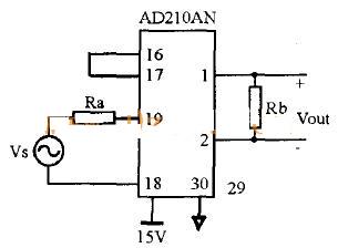
Figure 2 AD210 test principle diagram Figures 3 and 4 are the input and output voltage waveforms of the new circuit and AD210, respectively. The horizontal axis is time, and the vertical axis is the output voltage amplitude. It can be seen from the experiment that when the input frequency is 1 kHz, this isolation circuit and the integrated analog isolation amplifier AD210 have the same linearity and the same propagation delay. But at the high frequency end, the transmission delay of this circuit is much smaller than that of the integrated isolation amplifier circuit. It can be seen from Figure 3 that at 40kHz, the phase difference of this circuit is about 14 °. At this time, the output voltage and the input voltage are not distorted, and the transmission is linear. The propagation delay of the integrated analog isolation amplifier at 10 kHz is about 72 °. It can be seen that the transmission bandwidth of this isolation amplifier circuit is better than the integrated analog isolation amplifier.
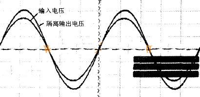
Figure 3 The input and output voltage waveform of this new circuit (fin is 40 kHz)
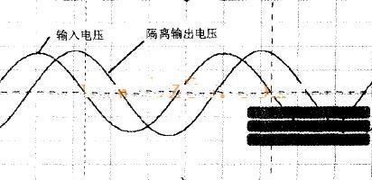
Figure 4 AD210 input and output voltage waveform (fin is 10 kHz)
Table 1 compares the performance of the isolation amplifier and the dedicated analog isolation amplifier AD210 and ISO124. 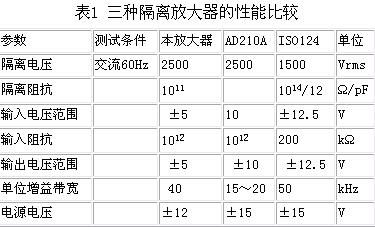
Among them, isolation voltage and isolation impedance are given parameters of optocoupler TLP521; input impedance, power supply voltage and input voltage range are given parameters of operational amplifier LF353; unity gain bandwidth and output voltage range are actual measured values.
As can be seen from Table 1, this isolation amplifier is the same as the integrated analog isolation amplifier in some respects (such as isolation voltage, input impedance). It is slightly worse than the integrated isolation amplifier in terms of small signal bandwidth and output voltage range. When the frequency increases, the output voltage amplitude increases is a problem that needs further study.
4 Conclusion This paper presents a new scheme to realize analog isolation amplifier circuit using four optocouplers. The circuit structure of the scheme is simple, easy to implement, and the price is low. Comparison experiments with the integrated analog isolation amplifier AD210 show that the performance of this isolation amplifier is excellent and has good application prospects.
Wire Feeding Hose is a very important part in the spraying.
Wire Feeding Hose
Wire Feeding Hose,Wire Cement Feeding Hose,Feeding Concrete Hose,Wire Reinforced Hose
Shaoxing Tianlong Tin Materials Co.,Ltd. , https://www.tianlongspray.com