Keyword: HDI PCB || Flexible PCB || Flex Rigid PCB || RF PCB || Halogen-Free PCB
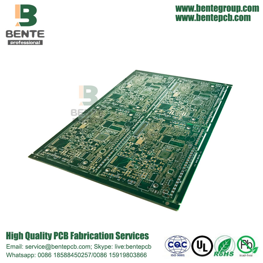
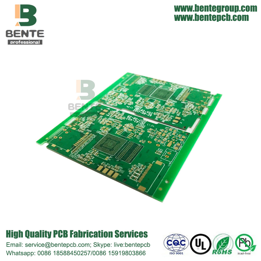
PCB market focus In recent years, the shift from computer to communication, mobile terminal with HDI board as the main point of PCB growth, mobile terminals represented by smart phones drive HDI board higher density and more light.
1, thin line
PCB all to high-density thin-line development, HDI board is particularly prominent. HDI was defined as a decade ago with a linewidth / pitch of 0.1 mm / 0.1 mm and below, and is now typically 60 μm in the industry and 40 μm advanced.

PCB line pattern formation, the traditional copper foil substrate after the optical imaging chemical etching process (subtraction method). This procedure and more control difficult and costly. The current fine line production tends to semi-additive method or improved semi-processed method.
2, semi-additive layer of substrate
Now semi-additive method is the use of insulating layer insulation film layer, from the fine line to achieve and make the cost of SAP is more favorable than MSAP. Layered with heat-curing resin, the laser drilled copper plated copper to form vias and circuit patterns.

At present, the international HDI laminated materials with epoxy resin with different curing agent to add inorganic powder to improve material rigidity and reduce CTE, but also the use of glass cloth to enhance rigidity.
Future trends. The carrier board will continue at fine BGA and CSP spacing, while coreless boards are more commonly used with carrier boards of four or more layers, the roadmap shows smaller feature sizes of carrier boards, lower performance requirements for critical dielectrics, lower dielectric Thermal expansion coefficient and high heat resistance, the pursuit of low-cost substrate to meet the performance goals.
PCB market focus In recent years, the shift from computer to communication, mobile terminal with HDI board as the main point of PCB growth, mobile terminals represented by smart phones drive HDI board higher density and more light.
1, thin line
PCB all to high-density thin-line development, HDI board is particularly prominent. HDI was defined as a decade ago with a linewidth / pitch of 0.1 mm / 0.1 mm and below, and is now typically 60 μm in the industry and 40 μm advanced.

PCB line pattern formation, the traditional copper foil substrate after the optical imaging chemical etching process (subtraction method). This procedure and more control difficult and costly. The current fine line production tends to semi-additive method or improved semi-processed method.
2, semi-additive layer of substrate
Now semi-additive method is the use of insulating layer insulation film layer, from the fine line to achieve and make the cost of SAP is more favorable than MSAP. Layered with heat-curing resin, the laser drilled copper plated copper to form vias and circuit patterns.

At present, the international HDI laminated materials with epoxy resin with different curing agent to add inorganic powder to improve material rigidity and reduce CTE, but also the use of glass cloth to enhance rigidity.
Future trends. The carrier board will continue at fine BGA and CSP spacing, while coreless boards are more commonly used with carrier boards of four or more layers, the roadmap shows smaller feature sizes of carrier boards, lower performance requirements for critical dielectrics, lower dielectric Thermal expansion coefficient and high heat resistance, the pursuit of low-cost substrate to meet the performance goals.