1 Introduction
The input part of the power supply, in order to prevent misoperation, the positive and negative poles of the power supply are reversed, causing damage to the circuit, generally it will be protected, such as the use of fuses, diodes, MOS tube, etc., here to do a little combing summary.
2, method:
2.1 Diode Reverse Connection
Diode protection is used, the circuit is simple, the cost is low, and the space is small. However, when the PN junction of the diode is turned on, there is a voltage drop of <= 0.7V, causing unnecessary losses to the circuit. For example, in a battery-powered system, a circuit with a large current will cause a significant effect (in circuit, Power consumption and heat are problems that cannot be ignored.)
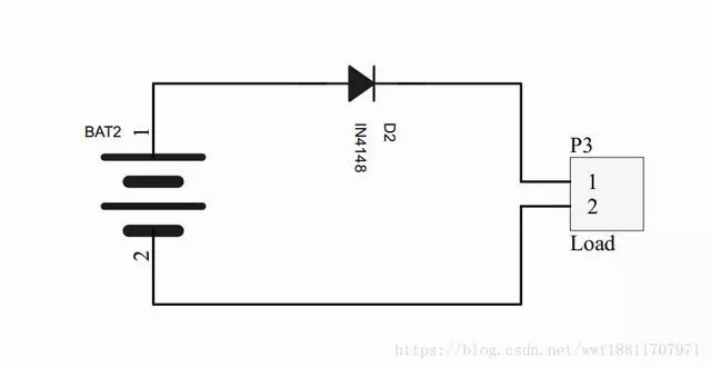
2.2 Fuse protection
Many common electronic products, after being disassembled, can see that the power supply part is fused. When the power supply is reversed, there is a short circuit in the circuit. Because of the large current, the fuse is blown to protect the circuit, but this way Repair and replacement are bothersome.
2.3 MOS tube protection
MOS tube due to process improvement, its own nature and other factors, its conduction resistance resistance technology school, many are milliohm level, or even smaller, so that the circuit voltage drop, power loss caused by the damage is particularly small, even negligible, so Selecting MOS transistors to protect the circuit is a recommended method.
2.3.1 NMOS protection
As shown below: At the moment of power-up, the parasitic diode of the MOS transistor turns on, and the system forms a loop. The potential of the source S is about 0.6V, and the potential of the gate G is Vbat, and the turn-on voltage of the MOS transistor is extremely high: Ugs = Vbat - Vs The gate shows a high level, the NMOS ds conducts, the parasitic diode is shorted, and the system forms a loop through the NMOS ds access.
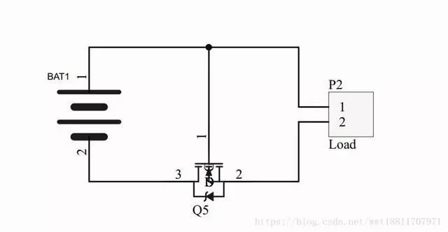
If the power is reversed, the NMOS's turn-on voltage is 0, the NMOS is turned off, the parasitic diode is reversed, and the circuit is disconnected, thus forming a protection.
2.3.2 PMOS protection
As shown below: At the instant of power-on, the parasitic diode of the MOS transistor turns on, and the system forms a loop. The potential of the source S is approximately Vbat-0.6V, and the potential of the gate G is 0, and the turn-on voltage of the MOS transistor is extremely high: Ugs = 0 - (Vbat-0.6), the gate shows a low level, the PMOS ds is turned on, the parasitic diode is short-circuited, and the system forms a loop through the PMOS ds access.
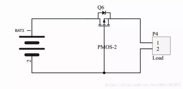
If the power is reversed, the NMOS's turn-on voltage is greater than zero, the PMOS is turned off, the parasitic diodes are reversed, and the circuit is disconnected, thereby creating protection.
Note: The NMOS transistor strings the ds string to the negative electrode, the PMOS transistor string to the positive electrode, and the direction of the parasitic diode is oriented in the direction of the correctly connected current.
Access of D and S poles of MOS transistors: When an N-channel MOS transistor is normally used, the current is usually entered from the D-pole and out of the S-pole, and the PMOS is the S-in and D-out. When applied in this circuit, it is exactly Instead, the MOS transistor is turned on by the conduction of the parasitic diode. As long as the MOS tube establishes a suitable voltage between the G and S poles, it will be completely turned on. After the turn-on, between D and S is like a switch is closed, the current is the same resistance from D to S or S to D.
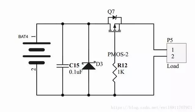
In practical applications, a resistance is generally connected in series with the G electrode. In order to prevent the MOS tube from being broken down, a Zener diode may be added. The capacitor connected in parallel on the voltage divider resistor has a soft start effect. At the instant that the current starts to flow, the capacitor is charged and the voltage at the G-pole is gradually established.
For PMOS, Vgs needs to be greater than the threshold voltage compared to the NOMS conduction, since its turn-on voltage can be 0, and the pressure difference between DS is not large, which is more advantageous than NMOS.
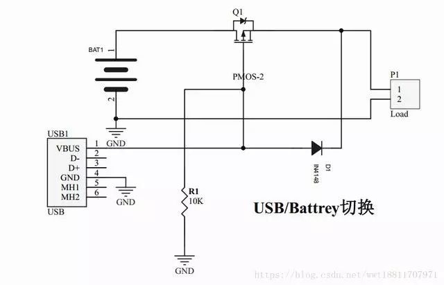
USB and battery switching design:
When the USB power supply, PMOS cut-off, through the diode input system; When the battery is powered, PMOS conduction, the role of the pull-down resistor is to stabilize the gate voltage is pulled low, to ensure the normal opening of the PMOS, to prevent the hidden dangers of high impedance gate .
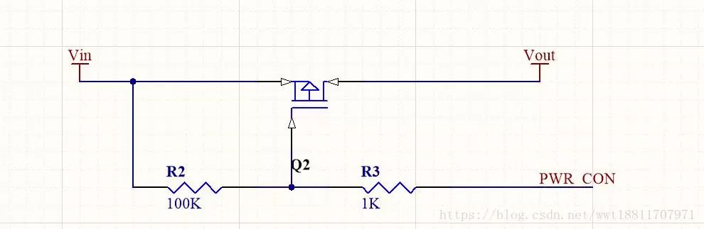
Through the MCU's IO control input -> output:
R3 ensures that the gate current is not too large, R2 pulls up, turns off PMOS, and the IO output is controlled, the stability is low, and the PMOS is turned on.
UL Metal Case Wide Voltage Led Driver
UL Metal Case Wide Voltage Led Driver
It is specially used in the US market, over UL certification, steel shell packaging, high safety performance, for panel lights, troffer indoor use, conventional products, stable quality, high PF value, 100-277 input, to avoid in high temperature and humid environment use.
Questions about flicker-free light may arise at this point. To be fair, it should be pointed out that fluorescent tubes operated with conventional or low loss ballast also flicker at 100 Hz and the light output is reduced at lower ambient temperatures. Fluorescent lamps operated with an ECG, including energy saving lamps, work at 44 – 50 kHz so that the lamps normally do not flicker. In reality, however, things are a little different. While a higher switching frequency is used, the input capacitors are to small for cost reasons. This causes the high frequency circuit in the lamp to be supplied with a strongly pulsating voltage. This pulsation creates a brightness modulation in the emitted light which is why these lamps often have a rather high level of flicker at 100 Hz.
Led Driver 50-70V,Constant Current Led Driver Pf,Driver For Led Panel Lights
ShenZhen Fahold Electronic Limited , https://www.fahold.net